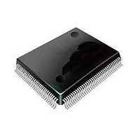
ST92F120V1Q7 STMicroelectronics, ST92F120V1Q7 Datasheet - Page 90

ST92F120V1Q7
Manufacturer Part Number
ST92F120V1Q7
Description
Microcontrollers (MCU) Flash 128K SPI/I2C
Manufacturer
STMicroelectronics
Datasheet
1.ST92F120V9Q7.pdf
(325 pages)
Specifications of ST92F120V1Q7
Data Bus Width
8 bit, 16 bit
Program Memory Type
Flash
Program Memory Size
128 KB
Data Ram Size
4 KB
Interface Type
I2C, SPI
Maximum Clock Frequency
24 MHz
Number Of Programmable I/os
77
Number Of Timers
5
Maximum Operating Temperature
+ 105 C
Mounting Style
SMD/SMT
Package / Case
PQFP-100
Minimum Operating Temperature
- 40 C
On-chip Adc
8 bit, 16 Channel
Lead Free Status / Rohs Status
No
Available stocks
Company
Part Number
Manufacturer
Quantity
Price
Company:
Part Number:
ST92F120V1Q7
Manufacturer:
ST
Quantity:
6 765
Part Number:
ST92F120V1Q7
Manufacturer:
ST
Quantity:
20 000
Part Number:
ST92F120V1Q7C
Manufacturer:
ST
Quantity:
20 000
Company:
Part Number:
ST92F120V1Q7DTR
Manufacturer:
MAXIM
Quantity:
2 854
- Current page: 90 of 325
- Download datasheet (3Mb)
ST92F120 - ON-CHIP DIRECT MEMORY ACCESS (DMA)
6.3 DMA TRANSACTIONS
The purpose of an on-chip DMA channel is to
transfer a block of data between a peripheral and
the Register File, or Memory. Each DMA transfer
consists of three operations:
– A load from/to the peripheral data register to/
– A post-increment of the DMA Address Register
– A post-decrement of the DMA transaction coun-
If the DMA transaction is carried out between the
peripheral and the Register File
register is required to hold the DMA Address, and
one to hold the DMA transaction counter. These
two registers must be located in the Register File:
the DMA Address Register in the even address
Figure 41. DMA Between Register File and Peripheral
90/324
9
from a location of Register File (or Memory) ad-
dressed through the DMA Address Register (or
Register pair)
(or Register pair)
ter, which contains the number of transactions
that have still to be performed.
PAGED REGISTERS
PERIPHERAL
DAPR
DCPR
DATA
IDCR
IVR
TABLE
DMA
FFh
F0h
EFh
E0h
DFh
(Figure
TRANSFERRED
REGISTER FILE
REGISTERS
REGISTERS
COUNTER
ADDRESS
ALREADY
41), one
SYSTEM
PAGED
DMA
DATA
DMA
register, and the DMA Transaction Counter in the
next register (odd address). They are pointed to by
the DMA Transaction Counter Pointer Register
(DCPR), located in the peripheral’s paged regis-
ters. In order to select a DMA transaction with the
Register File, the control bit DCPR.RM (bit 0 of
DCPR) must be set.
If the transaction is made between the peripheral
and Memory, a register pair (16 bits) is required
for the DMA Address and the DMA Transaction
Counter
be located in the Register File.
The DMA Transaction Counter is pointed to by the
DMA
(DCPR), the DMA Address is pointed to by the
DMA Address Pointer Register (DAPR),both
DCPR and DAPR are located in the paged regis-
ters of the peripheral.
000000h
000100h
Transaction
(Figure
SERVICE ROUTINE
END OF BLOCK
42). Thus, two register pairs must
ISR ADDRESS
INTERRUPT
MEMORY
Counter
Pointer
VECTOR
Register
TABLE
Related parts for ST92F120V1Q7
Image
Part Number
Description
Manufacturer
Datasheet
Request
R

Part Number:
Description:
8/16-bit Flash Mcu Family With Ram, Eeprom And J1850 Blpd
Manufacturer:
STMicroelectronics
Datasheet:

Part Number:
Description:
STMicroelectronics [RIPPLE-CARRY BINARY COUNTER/DIVIDERS]
Manufacturer:
STMicroelectronics
Datasheet:

Part Number:
Description:
STMicroelectronics [LIQUID-CRYSTAL DISPLAY DRIVERS]
Manufacturer:
STMicroelectronics
Datasheet:

Part Number:
Description:
BOARD EVAL FOR MEMS SENSORS
Manufacturer:
STMicroelectronics
Datasheet:

Part Number:
Description:
NPN TRANSISTOR POWER MODULE
Manufacturer:
STMicroelectronics
Datasheet:

Part Number:
Description:
TURBOSWITCH ULTRA-FAST HIGH VOLTAGE DIODE
Manufacturer:
STMicroelectronics
Datasheet:

Part Number:
Description:
Manufacturer:
STMicroelectronics
Datasheet:

Part Number:
Description:
DIODE / SCR MODULE
Manufacturer:
STMicroelectronics
Datasheet:

Part Number:
Description:
DIODE / SCR MODULE
Manufacturer:
STMicroelectronics
Datasheet:

Part Number:
Description:
Search -----> STE16N100
Manufacturer:
STMicroelectronics
Datasheet:

Part Number:
Description:
Search ---> STE53NA50
Manufacturer:
STMicroelectronics
Datasheet:

Part Number:
Description:
NPN Transistor Power Module
Manufacturer:
STMicroelectronics
Datasheet:


