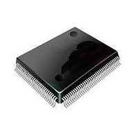
ST92F120V1Q7 STMicroelectronics, ST92F120V1Q7 Datasheet - Page 258

ST92F120V1Q7
Manufacturer Part Number
ST92F120V1Q7
Description
Microcontrollers (MCU) Flash 128K SPI/I2C
Manufacturer
STMicroelectronics
Datasheet
1.ST92F120V9Q7.pdf
(325 pages)
Specifications of ST92F120V1Q7
Data Bus Width
8 bit, 16 bit
Program Memory Type
Flash
Program Memory Size
128 KB
Data Ram Size
4 KB
Interface Type
I2C, SPI
Maximum Clock Frequency
24 MHz
Number Of Programmable I/os
77
Number Of Timers
5
Maximum Operating Temperature
+ 105 C
Mounting Style
SMD/SMT
Package / Case
PQFP-100
Minimum Operating Temperature
- 40 C
On-chip Adc
8 bit, 16 Channel
Lead Free Status / Rohs Status
No
Available stocks
Company
Part Number
Manufacturer
Quantity
Price
Company:
Part Number:
ST92F120V1Q7
Manufacturer:
ST
Quantity:
6 765
Part Number:
ST92F120V1Q7
Manufacturer:
ST
Quantity:
20 000
Part Number:
ST92F120V1Q7C
Manufacturer:
ST
Quantity:
20 000
Company:
Part Number:
ST92F120V1Q7DTR
Manufacturer:
MAXIM
Quantity:
2 854
- Current page: 258 of 325
- Download datasheet (3Mb)
J1850 Byte Level Protocol Decoder (JBLPD)
J1850 BYTE LEVEL PROTOCOL DECODER (Cont’d)
10.8.7 Register Description
The JBLPD peripheral uses 48 registers that are
mapped in a single page of the ST9 register file.
Twelve registers are mapped from R240 (F0h) to
R251 (FBh): these registers are usually used to
control the JBLPD. See
Stacked Registers
these registers.
Thirty-six registers are mapped from R252 (FCh)
to R255 (FFh). This is obtained by creating 9 sub-
pages, each containing 4 registers, mapped in the
same register addresses; 4 bits (RSEL[3:0]) of a
Figure 120. JBLPD Register Map
258/324
9
R241 (F1h)
R242 (F2h)
R243 (F3h)
R245 (F5h)
R246 (F6h)
R247 (F7h)
R249 (F9h)
R250 (FAh)
R251 (FBh)
R253 (FDh)
R254 (FEh)
R255 (FFh)
R240 (F0h)
R244 (F4h)
R248 (F8h)
R252 (FCh)
STATUS
PRLR
TXDATA
RXDATA
TXOP
CLKSEL
CONTROL
PADDR
ERROR
IVR
IMR
OPTIONS
CREG0
CREG1
CREG2
CREG3
for a detailed description of
Section 0.1.7.1 Un-
RDAPR
RDCPR
TDAPR
TDCPR
FREG0
FREG1
FREG2
FREG3
FREG4
FREG5
FREG6
FREG7
register (OPTIONS) are used to select the current
sub-page. See
section for a detailed description of these regis-
ters.
The ST9 Register File page used is 23 (17h).
NOTE: Bits marked as “Reserved” should be left at
their reset value to guarantee software compatibil-
ity with future versions of the JBLPD.
FREG8
FREG9
FREG10
FREG11
FREG12
FREG13
FREG14
FREG15
Section 0.1.7.2 Stacked Registers
FREG16
FREG17
FREG18
FREG19
FREG20
FREG21
FREG22
FREG23
FREG24
FREG25
FREG26
FREG27
FREG29
FREG28
FREG30
FREG31
Related parts for ST92F120V1Q7
Image
Part Number
Description
Manufacturer
Datasheet
Request
R

Part Number:
Description:
8/16-bit Flash Mcu Family With Ram, Eeprom And J1850 Blpd
Manufacturer:
STMicroelectronics
Datasheet:

Part Number:
Description:
STMicroelectronics [RIPPLE-CARRY BINARY COUNTER/DIVIDERS]
Manufacturer:
STMicroelectronics
Datasheet:

Part Number:
Description:
STMicroelectronics [LIQUID-CRYSTAL DISPLAY DRIVERS]
Manufacturer:
STMicroelectronics
Datasheet:

Part Number:
Description:
BOARD EVAL FOR MEMS SENSORS
Manufacturer:
STMicroelectronics
Datasheet:

Part Number:
Description:
NPN TRANSISTOR POWER MODULE
Manufacturer:
STMicroelectronics
Datasheet:

Part Number:
Description:
TURBOSWITCH ULTRA-FAST HIGH VOLTAGE DIODE
Manufacturer:
STMicroelectronics
Datasheet:

Part Number:
Description:
Manufacturer:
STMicroelectronics
Datasheet:

Part Number:
Description:
DIODE / SCR MODULE
Manufacturer:
STMicroelectronics
Datasheet:

Part Number:
Description:
DIODE / SCR MODULE
Manufacturer:
STMicroelectronics
Datasheet:

Part Number:
Description:
Search -----> STE16N100
Manufacturer:
STMicroelectronics
Datasheet:

Part Number:
Description:
Search ---> STE53NA50
Manufacturer:
STMicroelectronics
Datasheet:

Part Number:
Description:
NPN Transistor Power Module
Manufacturer:
STMicroelectronics
Datasheet:


