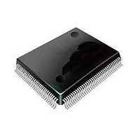
ST92F120V1Q7 STMicroelectronics, ST92F120V1Q7 Datasheet - Page 42

ST92F120V1Q7
Manufacturer Part Number
ST92F120V1Q7
Description
Microcontrollers (MCU) Flash 128K SPI/I2C
Manufacturer
STMicroelectronics
Datasheet
1.ST92F120V9Q7.pdf
(325 pages)
Specifications of ST92F120V1Q7
Data Bus Width
8 bit, 16 bit
Program Memory Type
Flash
Program Memory Size
128 KB
Data Ram Size
4 KB
Interface Type
I2C, SPI
Maximum Clock Frequency
24 MHz
Number Of Programmable I/os
77
Number Of Timers
5
Maximum Operating Temperature
+ 105 C
Mounting Style
SMD/SMT
Package / Case
PQFP-100
Minimum Operating Temperature
- 40 C
On-chip Adc
8 bit, 16 Channel
Lead Free Status / Rohs Status
No
Available stocks
Company
Part Number
Manufacturer
Quantity
Price
Company:
Part Number:
ST92F120V1Q7
Manufacturer:
ST
Quantity:
6 765
Part Number:
ST92F120V1Q7
Manufacturer:
ST
Quantity:
20 000
Part Number:
ST92F120V1Q7C
Manufacturer:
ST
Quantity:
20 000
Company:
Part Number:
ST92F120V1Q7DTR
Manufacturer:
MAXIM
Quantity:
2 854
- Current page: 42 of 325
- Download datasheet (3Mb)
ST92F120 - SINGLE VOLTAGE FLASH & EEPROM
3.3 REGISTER DESCRIPTION
3.3.1 Control Registers
FLASH CONTROL REGISTER (FCR)
Address: 224000h - Read/Write
Reset value: 0000 0000 (00h)
The Flash Control Register is used to enable all
the operations for the Flash and the TestFlash
memories. The write access to the TestFlash is
possible only in Test mode, except the OTP area
of the TestFlash that can be programmed in user
mode (but not erased).
Bit 7 = FWMS: Flash Write Mode Start (Read/
Write).
This bit must be set to start every write/erase oper-
ation in Flash memory. At the end of the write/
erase operation or during a Sector Erase Suspend
this bit is automatically reset. To resume a sus-
pended Sector Erase operation, this bit must be
set again. Resetting this bit by software does not
stop the current write operation.
0: No effect
1: Start Flash write
Bit 6 = FPAGE: Flash Page program (Read/Write) .
This bit must be set to select the Page Program
operation in Flash memory. The Page Program
operation allows to program “0”s in place of “1”s.
From 1 to 16 bytes can be entered (in any order,
no need for an ordered address sequence) before
starting the execution by setting the FWMS bit . All
the addresses must belong to the same page (only
the 4 LSBs of address can change). Data to be
programmed and addresses in which to program
must be provided (through an LD instruction, for
example). Data contained in page addresses that
are not entered are left unchanged. This bit is au-
tomatically reset at the end of the Page Program
operation.
0: Deselect page program
1: Select page program
Bit 5 = FCHIP: Flash CHIP erase (Read/Write).
This bit must be set to select the Chip Erase oper-
42/324
9
FWM
S
7
FPAG
E
6
FCHI
P
5
FBYT
E
4
FSEC
3
T
FSUS
P
2
PROT
1
FBUS
0
Y
ation in Flash memory. The Chip Erase operation
allows to erase all the Flash locations to FFh. The
operation is limited to Flash code (sectors F0-F3;
TestFlash and EEPROM sectors excluded). The
execution starts by setting the FWMS bit. It is not
necessary to pre-program the sectors to 00h, be-
cause this is done automatically. This bit is auto-
matically reset at the end of the Chip Erase opera-
tion.
0: Deselect chip erase
1: Select chip erase
Bit 4 = FBYTE: Flash byte program (Read/Write).
This bit must be set to select the Byte Program op-
eration in Flash memory. The Byte Program oper-
ation allows “0”s to be programmedin place of “1”s.
Data to be programmed and an address in which
to program must be provided (through an LD in-
struction, for example) before starting execution
by setting bit FWMS. This bit is automatically reset
at the end of the Byte Program operation.
0: Deselect byte program
1: Select byte program
Bit 3 = FSECT: Flash sector erase (Read/Write).
This bit must be set to select the Sector Erase op-
eration in Flash memory. The Sector Erase opera-
tion erases all the Flash locations to FFh. From 1
to 4 sectors (F0, ..,F3) can be simultaneously
erased, while TF must be individually erased. Sec-
tors to be simultaneously erased can be entered
before starting the execution by setting the FWMS
bit. An address located in the sector to erase must
be provided (through an LD instruction, for exam-
ple), while the data to be provided is don’t care. It
is not necessary to pre-program the sectors to
00h, because this is done automatically. This bit is
automatically reset at the end of the Sector Erase
operation.
0: Deselect sector erase
1: Select sector erase
Bit 2 = FSUSP: Flash sector erase suspend
(Read/Write) .
This bit must be set to suspend the current Sector
Erase operation in Flash memory in order to read
data to or from program data to a sector not being
erased. The Erase Suspend operation resets the
Flash memory to normal read mode (automatically
resetting bit FBUSY) in a maximum time of 15 s.
Related parts for ST92F120V1Q7
Image
Part Number
Description
Manufacturer
Datasheet
Request
R

Part Number:
Description:
8/16-bit Flash Mcu Family With Ram, Eeprom And J1850 Blpd
Manufacturer:
STMicroelectronics
Datasheet:

Part Number:
Description:
STMicroelectronics [RIPPLE-CARRY BINARY COUNTER/DIVIDERS]
Manufacturer:
STMicroelectronics
Datasheet:

Part Number:
Description:
STMicroelectronics [LIQUID-CRYSTAL DISPLAY DRIVERS]
Manufacturer:
STMicroelectronics
Datasheet:

Part Number:
Description:
BOARD EVAL FOR MEMS SENSORS
Manufacturer:
STMicroelectronics
Datasheet:

Part Number:
Description:
NPN TRANSISTOR POWER MODULE
Manufacturer:
STMicroelectronics
Datasheet:

Part Number:
Description:
TURBOSWITCH ULTRA-FAST HIGH VOLTAGE DIODE
Manufacturer:
STMicroelectronics
Datasheet:

Part Number:
Description:
Manufacturer:
STMicroelectronics
Datasheet:

Part Number:
Description:
DIODE / SCR MODULE
Manufacturer:
STMicroelectronics
Datasheet:

Part Number:
Description:
DIODE / SCR MODULE
Manufacturer:
STMicroelectronics
Datasheet:

Part Number:
Description:
Search -----> STE16N100
Manufacturer:
STMicroelectronics
Datasheet:

Part Number:
Description:
Search ---> STE53NA50
Manufacturer:
STMicroelectronics
Datasheet:

Part Number:
Description:
NPN Transistor Power Module
Manufacturer:
STMicroelectronics
Datasheet:


