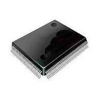
ST92F120V1Q7 STMicroelectronics, ST92F120V1Q7 Datasheet - Page 117

ST92F120V1Q7
Manufacturer Part Number
ST92F120V1Q7
Description
Microcontrollers (MCU) Flash 128K SPI/I2C
Manufacturer
STMicroelectronics
Datasheet
1.ST92F120V9Q7.pdf
(325 pages)
Specifications of ST92F120V1Q7
Data Bus Width
8 bit, 16 bit
Program Memory Type
Flash
Program Memory Size
128 KB
Data Ram Size
4 KB
Interface Type
I2C, SPI
Maximum Clock Frequency
24 MHz
Number Of Programmable I/os
77
Number Of Timers
5
Maximum Operating Temperature
+ 105 C
Mounting Style
SMD/SMT
Package / Case
PQFP-100
Minimum Operating Temperature
- 40 C
On-chip Adc
8 bit, 16 Channel
Lead Free Status / Rohs Status
No
Available stocks
Company
Part Number
Manufacturer
Quantity
Price
Company:
Part Number:
ST92F120V1Q7
Manufacturer:
ST
Quantity:
6 765
Part Number:
ST92F120V1Q7
Manufacturer:
ST
Quantity:
20 000
Part Number:
ST92F120V1Q7C
Manufacturer:
ST
Quantity:
20 000
Company:
Part Number:
ST92F120V1Q7DTR
Manufacturer:
MAXIM
Quantity:
2 854
- Current page: 117 of 325
- Download datasheet (3Mb)
EXTERNAL MEMORY INTERFACE REGISTERS (Cont’d)
Bits 1:0 = UAS[1:0]: Upper memory address
strobe stretch .
These two bits contain the number of wait cycles
(from 0 to 3) to add to the System Clock to stretch
AS during external upper memory block accesses
(MSB of 22-bit internal address=1). The reset val-
ue is 3.
CAUTION: The EMR2 register cannot be written
during an interrupt service routine.
WAIT CONTROL REGISTER (WCR)
R252 - Read/Write
Register Page: 0
Reset Value: 0111 1111 (7Fh)
Bit 7 = Reserved, forced by hardware to 0.
Bit 6 = WDGEN: Watchdog Enable.
For a description of this bit, refer to the Timer/
Watchdog chapter.
CAUTION: Clearing this bit has the effect of set-
ting the Timer/Watchdog to Watchdog mode. Un-
less this is desired, it must be set to “1”.
Bits 5:3 = UDS[2:0]: Upper memory data strobe
stretch.
These bits contain the number of INTCLK cycles
to be added automatically to DS for external upper
memory block accesses. UDS = 0 adds no addi-
7
0
WDGEN UDS2
UDS1
UDS0
LDS2
ST92F120 - EXTERNAL MEMORY INTERFACE (EXTMI)
LDS1 LDS0
0
tional wait cycles. UDS = 7 adds the maximum 7
INTCLK cycles (reset condition).
Bits 2:0 = LDS[2:0]: Lower memory data strobe
stretch.
These bits contain the number of INTCLK cycles
to be added automatically to DS or DS2 (depend-
ing on the DS2EN bit of the EMR1 register) for ex-
ternal lower memory block accesses. LDS = 0
adds no additional wait cycles, LDS = 7 adds the
maximum 7 INTCLK cycles (reset condition).
Note 1: The number of clock cycles added refers
to INTCLK and NOT to CPUCLK.
Note 2: The distinction between the Upper memo-
ry block and the Lower memory block allows differ-
ent wait cycles between the first 2 Mbytes and the
second 2 Mbytes, and allows 2 different data
strobe signals to be used to access 2 different
memories.
Typically, the RAM will be located above address
0x200000
0x1FFFFF, with different access times. No extra
hardware is required as DS is used to access the
upper memory block and DS2 is used to access
the lower memory block.
CAUTION : The reset value of the Wait Control
Register gives the maximum number of Wait cy-
cles for external memory. To get optimum perfor-
mance from the ST9, the user should write the
UDS[2:0] and LDS[2:0] bits to 0, if the external ad-
dressed memories are fast enough.
and
the
ROM
below
address
117/324
9
Related parts for ST92F120V1Q7
Image
Part Number
Description
Manufacturer
Datasheet
Request
R

Part Number:
Description:
8/16-bit Flash Mcu Family With Ram, Eeprom And J1850 Blpd
Manufacturer:
STMicroelectronics
Datasheet:

Part Number:
Description:
STMicroelectronics [RIPPLE-CARRY BINARY COUNTER/DIVIDERS]
Manufacturer:
STMicroelectronics
Datasheet:

Part Number:
Description:
STMicroelectronics [LIQUID-CRYSTAL DISPLAY DRIVERS]
Manufacturer:
STMicroelectronics
Datasheet:

Part Number:
Description:
BOARD EVAL FOR MEMS SENSORS
Manufacturer:
STMicroelectronics
Datasheet:

Part Number:
Description:
NPN TRANSISTOR POWER MODULE
Manufacturer:
STMicroelectronics
Datasheet:

Part Number:
Description:
TURBOSWITCH ULTRA-FAST HIGH VOLTAGE DIODE
Manufacturer:
STMicroelectronics
Datasheet:

Part Number:
Description:
Manufacturer:
STMicroelectronics
Datasheet:

Part Number:
Description:
DIODE / SCR MODULE
Manufacturer:
STMicroelectronics
Datasheet:

Part Number:
Description:
DIODE / SCR MODULE
Manufacturer:
STMicroelectronics
Datasheet:

Part Number:
Description:
Search -----> STE16N100
Manufacturer:
STMicroelectronics
Datasheet:

Part Number:
Description:
Search ---> STE53NA50
Manufacturer:
STMicroelectronics
Datasheet:

Part Number:
Description:
NPN Transistor Power Module
Manufacturer:
STMicroelectronics
Datasheet:


