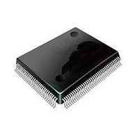
ST92F120V1Q7 STMicroelectronics, ST92F120V1Q7 Datasheet - Page 303

ST92F120V1Q7
Manufacturer Part Number
ST92F120V1Q7
Description
Microcontrollers (MCU) Flash 128K SPI/I2C
Manufacturer
STMicroelectronics
Datasheet
1.ST92F120V9Q7.pdf
(325 pages)
Specifications of ST92F120V1Q7
Data Bus Width
8 bit, 16 bit
Program Memory Type
Flash
Program Memory Size
128 KB
Data Ram Size
4 KB
Interface Type
I2C, SPI
Maximum Clock Frequency
24 MHz
Number Of Programmable I/os
77
Number Of Timers
5
Maximum Operating Temperature
+ 105 C
Mounting Style
SMD/SMT
Package / Case
PQFP-100
Minimum Operating Temperature
- 40 C
On-chip Adc
8 bit, 16 Channel
Lead Free Status / Rohs Status
No
Available stocks
Company
Part Number
Manufacturer
Quantity
Price
Company:
Part Number:
ST92F120V1Q7
Manufacturer:
ST
Quantity:
6 765
Part Number:
ST92F120V1Q7
Manufacturer:
ST
Quantity:
20 000
Part Number:
ST92F120V1Q7C
Manufacturer:
ST
Quantity:
20 000
Company:
Part Number:
ST92F120V1Q7DTR
Manufacturer:
MAXIM
Quantity:
2 854
- Current page: 303 of 325
- Download datasheet (3Mb)
SPI TIMING TABLE
(V
Note:
Measurement points are V
(1) Values guaranteed by design.
Legend:
Tck = INTCLK period = OSCIN period when OSCIN is not divided by 2;
N
10
11
12
13
1
2
3
4
5
6
7
8
9
DD
Symbol
= 5V
t
t
t
SPI_H
t
SPI_L
t
f
t
t
t
Lead
t
t
Hold
Rise
Lag
SPI
SPI
Fall
SU
t
Dis
t
t
H
A
V
10%, T
SPI frequency
SPI clock period
Enable lead time
Enable lag time
Clock (SCK) high time
Clock (SCK) low time
Data set-up time
Data hold time (inputs)
Access time (time to data active
from high impedance state)
Disable time (hold time to high im-
pedance state)
Data valid
Data hold time (outputs)
Rise time
(20% V
Fall time
(70% V
2 x OSCIN period when OSCIN is divided by 2;
OSCIN period x PLL factor when the PLL is enabled.
A
OL
DD
DD
=
, V
to 70% V
to 20% V
–
OH
Parameter
40°C to +105°C, C
, V
IL
and V
DD
DD
, C
, C
IH
L
L
in the SPI Timing Diagram.
= 200pF)
= 200pF)
Load
Master
Slave
Master
Slave
Slave
Slave
Master
Slave
Master
Slave
Master
Slave
Master
Slave
Slave
Master (before capture edge)
Slave (after enable edge)
Master (before capture edge)
Slave (after enable edge)
Outputs: SCK,MOSI,MISO
Inputs: SCK,MOSI,MISO,SS
Outputs: SCK,MOSI,MISO
Inputs: SCK,MOSI,MISO,SS
= 50pF, f
ST92F120 - ELECTRICAL CHARACTERISTICS
Condition
INTCLK
= 24MHz, unless otherwise specified)
f
INTCLK
4 x Tck
2 x Tck
Tck / 4
Tck / 4
Min
40
40
80
90
80
90
40
40
40
40
0
0
0
/ 128
Value
(1)
f
f
INTCLK
INTCLK
Max
120
240
120
100
100
100
100
/ 4
/ 2
303/324
MHz
Unit
ns
ns
ns
ns
ns
ns
ns
ns
ns
ns
ns
ns
ns
ns
ns
s
s
1
Related parts for ST92F120V1Q7
Image
Part Number
Description
Manufacturer
Datasheet
Request
R

Part Number:
Description:
8/16-bit Flash Mcu Family With Ram, Eeprom And J1850 Blpd
Manufacturer:
STMicroelectronics
Datasheet:

Part Number:
Description:
STMicroelectronics [RIPPLE-CARRY BINARY COUNTER/DIVIDERS]
Manufacturer:
STMicroelectronics
Datasheet:

Part Number:
Description:
STMicroelectronics [LIQUID-CRYSTAL DISPLAY DRIVERS]
Manufacturer:
STMicroelectronics
Datasheet:

Part Number:
Description:
BOARD EVAL FOR MEMS SENSORS
Manufacturer:
STMicroelectronics
Datasheet:

Part Number:
Description:
NPN TRANSISTOR POWER MODULE
Manufacturer:
STMicroelectronics
Datasheet:

Part Number:
Description:
TURBOSWITCH ULTRA-FAST HIGH VOLTAGE DIODE
Manufacturer:
STMicroelectronics
Datasheet:

Part Number:
Description:
Manufacturer:
STMicroelectronics
Datasheet:

Part Number:
Description:
DIODE / SCR MODULE
Manufacturer:
STMicroelectronics
Datasheet:

Part Number:
Description:
DIODE / SCR MODULE
Manufacturer:
STMicroelectronics
Datasheet:

Part Number:
Description:
Search -----> STE16N100
Manufacturer:
STMicroelectronics
Datasheet:

Part Number:
Description:
Search ---> STE53NA50
Manufacturer:
STMicroelectronics
Datasheet:

Part Number:
Description:
NPN Transistor Power Module
Manufacturer:
STMicroelectronics
Datasheet:


