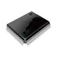
ST92F120V1Q7 STMicroelectronics, ST92F120V1Q7 Datasheet - Page 285

ST92F120V1Q7
Manufacturer Part Number
ST92F120V1Q7
Description
Microcontrollers (MCU) Flash 128K SPI/I2C
Manufacturer
STMicroelectronics
Datasheet
1.ST92F120V9Q7.pdf
(325 pages)
Specifications of ST92F120V1Q7
Data Bus Width
8 bit, 16 bit
Program Memory Type
Flash
Program Memory Size
128 KB
Data Ram Size
4 KB
Interface Type
I2C, SPI
Maximum Clock Frequency
24 MHz
Number Of Programmable I/os
77
Number Of Timers
5
Maximum Operating Temperature
+ 105 C
Mounting Style
SMD/SMT
Package / Case
PQFP-100
Minimum Operating Temperature
- 40 C
On-chip Adc
8 bit, 16 Channel
Lead Free Status / Rohs Status
No
Available stocks
Company
Part Number
Manufacturer
Quantity
Price
Company:
Part Number:
ST92F120V1Q7
Manufacturer:
ST
Quantity:
6 765
Part Number:
ST92F120V1Q7
Manufacturer:
ST
Quantity:
20 000
Part Number:
ST92F120V1Q7C
Manufacturer:
ST
Quantity:
20 000
Company:
Part Number:
ST92F120V1Q7DTR
Manufacturer:
MAXIM
Quantity:
2 854
- Current page: 285 of 325
- Download datasheet (3Mb)
ANALOG TO DIGITAL CONVERTER (Cont’d)
CONTROL LOGIC REGISTER (CLR)
The Control Logic Register (CLR) manages the
A/D converter logic. Writing to this register will
cause the current conversion to be aborted and
the autoscan logic to be re-initialized.
CONTROL LOGIC REGISTER (CLR)
R253 - Read/Write
Register Page: 63
Reset Value: 0000 0000 (00h)
Bit 7:5 = SC[2:0]: Start Conversion Address .
These 3 bits define the starting analog input chan-
nel (Autoscan mode). The first channel addressed
by SC[2:0] is converted, then the channel number
is incremented for the successive conversion, until
channel 7 (111) is converted. When SC2, SC1 and
SC0 are all set, only channel 7 will be converted.
Bit 4 = EXTG: External Trigger Enable .
This bit is set and cleared by software.
0: External trigger disabled.
1: External trigger enabled. Allows a conversion
Bit 3 = INTG: Internal Trigger Enable .
This bit is set and cleared by software.
0: Internal trigger disabled.
1: Internal trigger enabled. Allows a conversion se-
Both External and Internal Trigger inputs are inter-
nally ORed, thus avoiding Hardware conflicts;
SC2
sequence to be started on the subsequent edge
of the external signal applied to the EXTRG pin
(when enabled as an Alternate Function).
quence to be started, synchronized by an inter-
nal signal (On-chip Event signal) from a Multi-
function Timer peripheral.
7
SC1
SC0
EXT
G
INTG POW
EIGHT-CHANNEL ANALOG TO DIGITAL CONVERTER (A/D)
CON
T
ST
0
however, the correct procedure is to enable only
one alternate synchronization input at a time.
Note: The effect of either synchronization mode is
to set the START/STOP bit, which is reset by hard-
ware when in SINGLE mode, at the end of each
sequence of conversions.
Requirements: The External Synchronisation In-
put must receive a low level pulse longer than an
INTCLK period and, for both External and On-Chip
Event synchronisation, the repetition period must
be greater than the time required for the selected
sequence of conversions.
Bit 2 = POW: Power Up/Power Down.
This bit is set and cleared by software.
0: Power down mode: all power-consuming logic is
1: Power up mode: the A/D converter logic and an-
Bit 1 = CONT: Continuous/Single .
0: Single Mode: a single sequence of conversions
1: Continuous Mode: the first sequence of conver-
Bit 0 = ST: Start/Stop.
0: Stop conversion. When the A/D converter is
1: Start a sequence of conversions.
disabled, thus selecting a low power idle mode.
alog circuitry is enabled.
is initiated whenever an external (or internal)
trigger occurs, or when the ST bit is set by soft-
ware.
sions is started, either by software (by setting
the ST bit), or by hardware (on an internal or ex-
ternal trigger, depending on the setting of the
INTG and EXTG bits); a continuous conversion
sequence is then initiated.
running in Single Mode, this bit is hardware re-
set at the end of a sequence of conversions.
285/324
9
Related parts for ST92F120V1Q7
Image
Part Number
Description
Manufacturer
Datasheet
Request
R

Part Number:
Description:
8/16-bit Flash Mcu Family With Ram, Eeprom And J1850 Blpd
Manufacturer:
STMicroelectronics
Datasheet:

Part Number:
Description:
STMicroelectronics [RIPPLE-CARRY BINARY COUNTER/DIVIDERS]
Manufacturer:
STMicroelectronics
Datasheet:

Part Number:
Description:
STMicroelectronics [LIQUID-CRYSTAL DISPLAY DRIVERS]
Manufacturer:
STMicroelectronics
Datasheet:

Part Number:
Description:
BOARD EVAL FOR MEMS SENSORS
Manufacturer:
STMicroelectronics
Datasheet:

Part Number:
Description:
NPN TRANSISTOR POWER MODULE
Manufacturer:
STMicroelectronics
Datasheet:

Part Number:
Description:
TURBOSWITCH ULTRA-FAST HIGH VOLTAGE DIODE
Manufacturer:
STMicroelectronics
Datasheet:

Part Number:
Description:
Manufacturer:
STMicroelectronics
Datasheet:

Part Number:
Description:
DIODE / SCR MODULE
Manufacturer:
STMicroelectronics
Datasheet:

Part Number:
Description:
DIODE / SCR MODULE
Manufacturer:
STMicroelectronics
Datasheet:

Part Number:
Description:
Search -----> STE16N100
Manufacturer:
STMicroelectronics
Datasheet:

Part Number:
Description:
Search ---> STE53NA50
Manufacturer:
STMicroelectronics
Datasheet:

Part Number:
Description:
NPN Transistor Power Module
Manufacturer:
STMicroelectronics
Datasheet:


