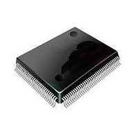
ST92F120V1Q7 STMicroelectronics, ST92F120V1Q7 Datasheet - Page 287

ST92F120V1Q7
Manufacturer Part Number
ST92F120V1Q7
Description
Microcontrollers (MCU) Flash 128K SPI/I2C
Manufacturer
STMicroelectronics
Datasheet
1.ST92F120V9Q7.pdf
(325 pages)
Specifications of ST92F120V1Q7
Data Bus Width
8 bit, 16 bit
Program Memory Type
Flash
Program Memory Size
128 KB
Data Ram Size
4 KB
Interface Type
I2C, SPI
Maximum Clock Frequency
24 MHz
Number Of Programmable I/os
77
Number Of Timers
5
Maximum Operating Temperature
+ 105 C
Mounting Style
SMD/SMT
Package / Case
PQFP-100
Minimum Operating Temperature
- 40 C
On-chip Adc
8 bit, 16 Channel
Lead Free Status / Rohs Status
No
Available stocks
Company
Part Number
Manufacturer
Quantity
Price
Company:
Part Number:
ST92F120V1Q7
Manufacturer:
ST
Quantity:
6 765
Part Number:
ST92F120V1Q7
Manufacturer:
ST
Quantity:
20 000
Part Number:
ST92F120V1Q7C
Manufacturer:
ST
Quantity:
20 000
Company:
Part Number:
ST92F120V1Q7DTR
Manufacturer:
MAXIM
Quantity:
2 854
- Current page: 287 of 325
- Download datasheet (3Mb)
11 ELECTRICAL CHARACTERISTICS
This product contains devices to protect the inputs
against damage due to high static voltages, how-
ever it is advisable to take normal precautions to
avoid application of any voltage higher than the
specified maximum rated voltages.
For proper operation it is recommended that V
and V
Reliability is enhanced if unused inputs are con-
nected to an appropriate logic voltage level (V
or V
ABSOLUTE MAXIMUM RATINGS
Note:
Stresses above those listed as “absolute maximum ratings“ may cause permanent damage to the device. This is a stress rating only and
functional operation of the device at these conditions is not implied. Exposure to maximum rating conditions for extended periods may affect
device reliability. All voltages are referenced to V
THERMAL CHARACTERISTICS
RECOMMENDED OPERATING CONDITIONS
Note:
(1) 1MHz when A/D or JBLPD is used, 2.6MHz when I²C is used.
Symbol
SS
Symbol
V
Symbol
AV
AV
f
T
V
ESD
V
RthJA
AV
INTCLK
I
V
INOD
O
STG
V
INJ
).
AIN
DD
T
IN
DD
SS
DD
A
be higher than V
DD
Supply Voltage
A/D Converter Analog Reference
A/D Converter V
Input Voltage (standard I/O pins)
Input Voltage (open drain I/O pins)
Analog Input Voltage (A/D Converter)
Storage Temperature
Pin Injection Current - Digital and Analog Input
Maximum Accumulated Pin injection Current in the device
ESD Susceptibility
Operating Temperature
Operating Supply Voltage
Analog Supply Voltage
Internal Clock Frequency @ 4.5V - 5.5V
SS
PQFP100
and lower than V
Package
SS
SS
Parameter
Parameter
=0.
DD
DD
IN
ST92F120 - ELECTRICAL CHARACTERISTICS
.
Power Considerations. The average chip-junc-
tion temperature, T
from:
Where: T
T
RthJA = Package thermal resistance
P
P
P
J
A
D
INT
PORT
=
=
Value
=
28
=
= Port power dissipation
V
(junction-to ambient).
(determined by the user)
T
Ambient Temperature.
P
I
V
DD
DD
A
DD
INT
Min
–40
0
– 0.3 to V
4.5
J
+ P
(1)
, in Celsius can be obtained
- 0.3
x V
AV
– 0.3 to V
– 55 to +150
+ P
– 0.3 to 6.5
– 0.3 to 6.5
Value
D
SS
DD
Value
2000
V
PORT
x RthJA
100
to AV
10
SS
V
(chip internal power).
DD
DD
Max
DD
105
5.5
24
+ 0.3
.
+ 0.3
DD
+ 0.3
Unit
C/W
MHz
Unit
V
V
Unit
287/324
C
mA
mA
V
V
V
V
V
V
C
1
Related parts for ST92F120V1Q7
Image
Part Number
Description
Manufacturer
Datasheet
Request
R

Part Number:
Description:
8/16-bit Flash Mcu Family With Ram, Eeprom And J1850 Blpd
Manufacturer:
STMicroelectronics
Datasheet:

Part Number:
Description:
STMicroelectronics [RIPPLE-CARRY BINARY COUNTER/DIVIDERS]
Manufacturer:
STMicroelectronics
Datasheet:

Part Number:
Description:
STMicroelectronics [LIQUID-CRYSTAL DISPLAY DRIVERS]
Manufacturer:
STMicroelectronics
Datasheet:

Part Number:
Description:
BOARD EVAL FOR MEMS SENSORS
Manufacturer:
STMicroelectronics
Datasheet:

Part Number:
Description:
NPN TRANSISTOR POWER MODULE
Manufacturer:
STMicroelectronics
Datasheet:

Part Number:
Description:
TURBOSWITCH ULTRA-FAST HIGH VOLTAGE DIODE
Manufacturer:
STMicroelectronics
Datasheet:

Part Number:
Description:
Manufacturer:
STMicroelectronics
Datasheet:

Part Number:
Description:
DIODE / SCR MODULE
Manufacturer:
STMicroelectronics
Datasheet:

Part Number:
Description:
DIODE / SCR MODULE
Manufacturer:
STMicroelectronics
Datasheet:

Part Number:
Description:
Search -----> STE16N100
Manufacturer:
STMicroelectronics
Datasheet:

Part Number:
Description:
Search ---> STE53NA50
Manufacturer:
STMicroelectronics
Datasheet:

Part Number:
Description:
NPN Transistor Power Module
Manufacturer:
STMicroelectronics
Datasheet:


