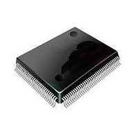
ST92F120V1Q7 STMicroelectronics, ST92F120V1Q7 Datasheet - Page 20

ST92F120V1Q7
Manufacturer Part Number
ST92F120V1Q7
Description
Microcontrollers (MCU) Flash 128K SPI/I2C
Manufacturer
STMicroelectronics
Datasheet
1.ST92F120V9Q7.pdf
(325 pages)
Specifications of ST92F120V1Q7
Data Bus Width
8 bit, 16 bit
Program Memory Type
Flash
Program Memory Size
128 KB
Data Ram Size
4 KB
Interface Type
I2C, SPI
Maximum Clock Frequency
24 MHz
Number Of Programmable I/os
77
Number Of Timers
5
Maximum Operating Temperature
+ 105 C
Mounting Style
SMD/SMT
Package / Case
PQFP-100
Minimum Operating Temperature
- 40 C
On-chip Adc
8 bit, 16 Channel
Lead Free Status / Rohs Status
No
Available stocks
Company
Part Number
Manufacturer
Quantity
Price
Company:
Part Number:
ST92F120V1Q7
Manufacturer:
ST
Quantity:
6 765
Part Number:
ST92F120V1Q7
Manufacturer:
ST
Quantity:
20 000
Part Number:
ST92F120V1Q7C
Manufacturer:
ST
Quantity:
20 000
Company:
Part Number:
ST92F120V1Q7DTR
Manufacturer:
MAXIM
Quantity:
2 854
- Current page: 20 of 325
- Download datasheet (3Mb)
ST92F120 - DEVICE ARCHITECTURE
2 DEVICE ARCHITECTURE
2.1 CORE ARCHITECTURE
The ST9 Core or Central Processing Unit (CPU)
features a highly optimised instruction set, capable
of handling bit, byte (8-bit) and word (16-bit) data,
as well as BCD and Boolean formats; 14 address-
ing modes are available.
Four independent buses are controlled by the
Core: a 16-bit Memory bus, an 8-bit Register data
bus, an 8-bit Register address bus and a 6-bit In-
terrupt/DMA bus which connects the interrupt and
DMA controllers in the on-chip peripherals with the
Core.
This multiple bus architecture affords a high de-
gree of pipelining and parallel operation, thus mak-
ing the ST9 family devices highly efficient, both for
numerical calculation, data handling and with re-
gard to communication with on-chip peripheral re-
sources.
2.2 MEMORY SPACES
There are two separate memory spaces:
– The Register File, which comprises 240 8-bit
Figure 9. Single Program and Data Memory Address Space
20/324
9
registers, arranged as 15 groups (Group 0 to E),
each containing sixteen 8-bit registers plus up to
64 pages of 16 registers mapped in Group F,
up to 4 Mbytes
Address
21FFFFh
210000h
20FFFFh
3FFFFFh
3F0000h
3EFFFFh
3E0000h
02FFFFh
020000h
01FFFFh
010000h
00FFFFh
000000h
Reserved
– A single linear memory space accommodating
2.2.1 Register File
The Register File consists of (see
– 224 general purpose registers (Group 0 to D,
– 6 system registers in the System Group (Group
– Up to 64 pages, depending on device configura-
which hold data and control bits for the on-chip
peripherals and I/Os.
both program and data. All of the physically sep-
arate memory areas, including the internal ROM,
internal RAM and external memory are mapped
in this common address space. The total ad-
dressable memory space of 4 Mbytes (limited by
the size of on-chip memory and the number of
external address pins) is arranged as 64 seg-
ments of 64 Kbytes. Each segment is further
subdivided into four pages of 16 Kbytes, as illus-
trated in
uses a set of pointer registers to address a 22-bit
memory field using 16-bit address-based instruc-
tions.
registers R0 to R223)
E, registers R224 to R239)
tion, each containing up to 16 registers, mapped
to Group F (R240 to R255), see
16K Pages
Data
255
254
253
252
251
250
249
248
247
135
134
133
132
11
10
9
8
7
6
5
4
3
2
1
0
Figure
64K Segments
1. A Memory Management Unit
Code
63
62
33
2
1
0
Figure
Figure
2):
3.
Related parts for ST92F120V1Q7
Image
Part Number
Description
Manufacturer
Datasheet
Request
R

Part Number:
Description:
8/16-bit Flash Mcu Family With Ram, Eeprom And J1850 Blpd
Manufacturer:
STMicroelectronics
Datasheet:

Part Number:
Description:
STMicroelectronics [RIPPLE-CARRY BINARY COUNTER/DIVIDERS]
Manufacturer:
STMicroelectronics
Datasheet:

Part Number:
Description:
STMicroelectronics [LIQUID-CRYSTAL DISPLAY DRIVERS]
Manufacturer:
STMicroelectronics
Datasheet:

Part Number:
Description:
BOARD EVAL FOR MEMS SENSORS
Manufacturer:
STMicroelectronics
Datasheet:

Part Number:
Description:
NPN TRANSISTOR POWER MODULE
Manufacturer:
STMicroelectronics
Datasheet:

Part Number:
Description:
TURBOSWITCH ULTRA-FAST HIGH VOLTAGE DIODE
Manufacturer:
STMicroelectronics
Datasheet:

Part Number:
Description:
Manufacturer:
STMicroelectronics
Datasheet:

Part Number:
Description:
DIODE / SCR MODULE
Manufacturer:
STMicroelectronics
Datasheet:

Part Number:
Description:
DIODE / SCR MODULE
Manufacturer:
STMicroelectronics
Datasheet:

Part Number:
Description:
Search -----> STE16N100
Manufacturer:
STMicroelectronics
Datasheet:

Part Number:
Description:
Search ---> STE53NA50
Manufacturer:
STMicroelectronics
Datasheet:

Part Number:
Description:
NPN Transistor Power Module
Manufacturer:
STMicroelectronics
Datasheet:


