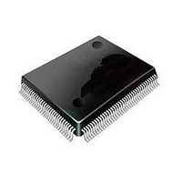
ST92F120V1Q7 STMicroelectronics, ST92F120V1Q7 Datasheet - Page 14

ST92F120V1Q7
Manufacturer Part Number
ST92F120V1Q7
Description
Microcontrollers (MCU) Flash 128K SPI/I2C
Manufacturer
STMicroelectronics
Datasheet
1.ST92F120V9Q7.pdf
(325 pages)
Specifications of ST92F120V1Q7
Data Bus Width
8 bit, 16 bit
Program Memory Type
Flash
Program Memory Size
128 KB
Data Ram Size
4 KB
Interface Type
I2C, SPI
Maximum Clock Frequency
24 MHz
Number Of Programmable I/os
77
Number Of Timers
5
Maximum Operating Temperature
+ 105 C
Mounting Style
SMD/SMT
Package / Case
PQFP-100
Minimum Operating Temperature
- 40 C
On-chip Adc
8 bit, 16 Channel
Lead Free Status / Rohs Status
No
Available stocks
Company
Part Number
Manufacturer
Quantity
Price
Company:
Part Number:
ST92F120V1Q7
Manufacturer:
ST
Quantity:
6 765
Part Number:
ST92F120V1Q7
Manufacturer:
ST
Quantity:
20 000
Part Number:
ST92F120V1Q7C
Manufacturer:
ST
Quantity:
20 000
Company:
Part Number:
ST92F120V1Q7DTR
Manufacturer:
MAXIM
Quantity:
2 854
- Current page: 14 of 325
- Download datasheet (3Mb)
ST92F120 - GENERAL DESCRIPTION
1.3 I/O PORTS
Port 0 and Port 1 provide the external memory in-
terface. All the ports of the device can be pro-
grammed as Input/Output or in Input mode, com-
patible with TTL or CMOS levels (except where
Schmitt Trigger is present). Each bit can be pro-
grammed individually (Refer to the I/O ports chap-
ter).
Internal Weak Pull-up
As shown in
ment a Weak Pull-up. This means that the pull-up
must be connected externally when the pin is not
used or programmed as bidirectional.
TTL/CMOS Input
For all those port bits where no input schmitt trig-
ger is implemented, it is always possible to pro-
gram the input level as TTL or CMOS compatible
by programming the relevant PxC2.n control bit.
Refer I/O Ports Chapter to the section titled “Input/
Output Bit Configuration”.
Schmitt Trigger Input
Two different kind of Schmitt Trigger circuitries are
implemented: Standard and High Hysteresis.
Standard Schmitt Trigger is widely used (see
ble
Table 3. I/O Port Characteristics
Legend: WPU = Weak Pull-Up, OD = Open Drain
14/324
9
Port 0[7:0]
Port 1[7:0]
Port 2[1:0]
Port 2[3:2]
Port 2[5:4]
Port 2[7:6]
Port 3[2:1]
Port 3.3
Port 3[7:4]
Port 4.0, Port 4.4
Port 4.1
Port 4.2, Port 4.5
Port 4.3
Port 4[7:6]
Port 5[2:0], Port 5[7:4]
Port 5.3
Port 6[3:0]
Port 6[5:4]
Port 7[7:0]
Port 8[1:0]
Port 8[7:2]
Port 9[7:0]
3), while the High Hysteresis one is present on
Table
3, not all input sections imple-
Input
TTL/CMOS
TTL/CMOS
Schmitt trigger
TTL/CMOS
Schmitt trigger
TTL/CMOS
Schmitt trigger
TTL/CMOS
Schmitt trigger
Schmitt trigger
Schmitt trigger
TTL/CMOS
Schmitt trigger
Schmitt trigger inside I/O cell
Schmitt trigger
TTL/CMOS
Schmitt trigger
High hysteresis Schmitt trigger
inside I/O cell
Schmitt trigger
Schmitt trigger
Schmitt trigger
Schmitt trigger
Ta-
Output
Push-Pull/OD
Push-Pull/OD
Push-Pull/OD
Pure OD
Push-Pull/OD
Push-Pull/OD
Push-Pull/OD
Push-Pull/OD
Push-Pull/OD
Push-Pull/OD
Push-Pull/OD
Push-Pull/OD
Push-Pull/OD
Pure OD
Push-Pull/OD
Push-Pull/OD
Push-Pull/OD
Push-Pull/OD
Push-Pull/OD
Push-Pull/OD
Push-Pull/OD
Push-Pull/OD
the NMI and VPWI input function pins mapped on
Port 6 [5:4] (see
All inputs which can be used for detecting interrupt
events have been configured with a “standard”
Schmitt Trigger, apart from, as already said, the
NMI pin which implements the “High Hysteresis”
version. In this way, all interrupt lines are guaran-
teed as “level sensitive”.
Push-Pull/OD Output
The output buffer can be programmed as push-
pull or open-drain: attention must be paid to the
fact that the open-drain option corresponds only to
a disabling of P-channel MOS transistor of the
buffer itself: it is still present and physically con-
nected to the pin. Consequently it is not possible to
increase the output voltage on the pin over
V
Pure Open-Drain Output
The user can increase the voltage on an I/O pin
over V
sistor is physically absent: this is allowed on all
“Pure Open Drain” pins. Of course, in this case the
push-pull option is not available and any weak
pull-up must implemented externally.
DD
+0.3 Volt, to avoid direct junction biasing.
DD
+0.3 Volt where the P-channel MOS tran-
Weak Pull-Up
No
No
Yes
No
Yes
Yes
Yes
Yes
Yes
No
Yes
Yes
Yes
No
No
Yes
Yes
Yes (inside I/O cell)
Yes
Yes
Yes
Yes
Table
4).
Reset State
Bidirectional
Bidirectional
Input
Input CMOS
Input
Input CMOS
Input
Input CMOS
Input
Input
Bidirectional WPU
Input CMOS
Input
Input
Input
Input CMOS
Input
Input
Input
Bidirectional WPU
Input
Bidirectional WPU
Related parts for ST92F120V1Q7
Image
Part Number
Description
Manufacturer
Datasheet
Request
R

Part Number:
Description:
8/16-bit Flash Mcu Family With Ram, Eeprom And J1850 Blpd
Manufacturer:
STMicroelectronics
Datasheet:

Part Number:
Description:
STMicroelectronics [RIPPLE-CARRY BINARY COUNTER/DIVIDERS]
Manufacturer:
STMicroelectronics
Datasheet:

Part Number:
Description:
STMicroelectronics [LIQUID-CRYSTAL DISPLAY DRIVERS]
Manufacturer:
STMicroelectronics
Datasheet:

Part Number:
Description:
BOARD EVAL FOR MEMS SENSORS
Manufacturer:
STMicroelectronics
Datasheet:

Part Number:
Description:
NPN TRANSISTOR POWER MODULE
Manufacturer:
STMicroelectronics
Datasheet:

Part Number:
Description:
TURBOSWITCH ULTRA-FAST HIGH VOLTAGE DIODE
Manufacturer:
STMicroelectronics
Datasheet:

Part Number:
Description:
Manufacturer:
STMicroelectronics
Datasheet:

Part Number:
Description:
DIODE / SCR MODULE
Manufacturer:
STMicroelectronics
Datasheet:

Part Number:
Description:
DIODE / SCR MODULE
Manufacturer:
STMicroelectronics
Datasheet:

Part Number:
Description:
Search -----> STE16N100
Manufacturer:
STMicroelectronics
Datasheet:

Part Number:
Description:
Search ---> STE53NA50
Manufacturer:
STMicroelectronics
Datasheet:

Part Number:
Description:
NPN Transistor Power Module
Manufacturer:
STMicroelectronics
Datasheet:


