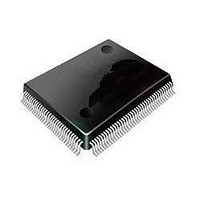
ST92F120V1Q7 STMicroelectronics, ST92F120V1Q7 Datasheet - Page 181

ST92F120V1Q7
Manufacturer Part Number
ST92F120V1Q7
Description
Microcontrollers (MCU) Flash 128K SPI/I2C
Manufacturer
STMicroelectronics
Datasheet
1.ST92F120V9Q7.pdf
(325 pages)
Specifications of ST92F120V1Q7
Data Bus Width
8 bit, 16 bit
Program Memory Type
Flash
Program Memory Size
128 KB
Data Ram Size
4 KB
Interface Type
I2C, SPI
Maximum Clock Frequency
24 MHz
Number Of Programmable I/os
77
Number Of Timers
5
Maximum Operating Temperature
+ 105 C
Mounting Style
SMD/SMT
Package / Case
PQFP-100
Minimum Operating Temperature
- 40 C
On-chip Adc
8 bit, 16 Channel
Lead Free Status / Rohs Status
No
Available stocks
Company
Part Number
Manufacturer
Quantity
Price
Company:
Part Number:
ST92F120V1Q7
Manufacturer:
ST
Quantity:
6 765
Part Number:
ST92F120V1Q7
Manufacturer:
ST
Quantity:
20 000
Part Number:
ST92F120V1Q7C
Manufacturer:
ST
Quantity:
20 000
Company:
Part Number:
ST92F120V1Q7DTR
Manufacturer:
MAXIM
Quantity:
2 854
- Current page: 181 of 325
- Download datasheet (3Mb)
MULTIPROTOCOL SERIAL COMMUNICATIONS INTERFACE (Cont’d)
10.5.4 SCI-M Operating Modes
10.5.4.1 Asynchronous Mode
In this mode, data and clock can be asynchronous
(the transmitter and receiver can use their own
clocks to sample received data), each data bit is
sampled 16 times per clock period.
The baud rate clock should be set to the ÷16 Mode
and the frequency of the input clock (from an ex-
ternal source or from the internal baud-rate gener-
ator output) is set to suit.
Figure 90. Sampling Times in Asynchronous Format
SDIN
rcvck
rxclk
LEGEND:
SIN:
rcvck:
rxd:
rxclk:
rxd
Serial Data Input line
Internal X16 Receiver Clock
Internal Serial Data Input Line
Internal Receiver Shift Register Sampling Clock
0
MULTIPROTOCOL SERIAL COMMUNICATIONS INTERFACE (SCI-M)
1
2
3
4
5
10.5.4.2
Synchronous Clock
In this mode, data and clock are synchronous,
each data bit is sampled once per clock period.
For transmit operation, a general purpose I/O port
pin can be programmed to output the CLKOUT
signal from the baud rate generator. If the SCI is
provided with an external transmission clock
source, there will be a skew equivalent to two
INTCLK periods between clock and data.
Data will be transmitted on the falling edge of the
transmit clock. Received data will be latched into
the SCI on the rising edge of the receive clock.
7
8
9
Asynchronous
10
11
12
13
14
Mode
15
VR001409
181/324
with
9
Related parts for ST92F120V1Q7
Image
Part Number
Description
Manufacturer
Datasheet
Request
R

Part Number:
Description:
8/16-bit Flash Mcu Family With Ram, Eeprom And J1850 Blpd
Manufacturer:
STMicroelectronics
Datasheet:

Part Number:
Description:
STMicroelectronics [RIPPLE-CARRY BINARY COUNTER/DIVIDERS]
Manufacturer:
STMicroelectronics
Datasheet:

Part Number:
Description:
STMicroelectronics [LIQUID-CRYSTAL DISPLAY DRIVERS]
Manufacturer:
STMicroelectronics
Datasheet:

Part Number:
Description:
BOARD EVAL FOR MEMS SENSORS
Manufacturer:
STMicroelectronics
Datasheet:

Part Number:
Description:
NPN TRANSISTOR POWER MODULE
Manufacturer:
STMicroelectronics
Datasheet:

Part Number:
Description:
TURBOSWITCH ULTRA-FAST HIGH VOLTAGE DIODE
Manufacturer:
STMicroelectronics
Datasheet:

Part Number:
Description:
Manufacturer:
STMicroelectronics
Datasheet:

Part Number:
Description:
DIODE / SCR MODULE
Manufacturer:
STMicroelectronics
Datasheet:

Part Number:
Description:
DIODE / SCR MODULE
Manufacturer:
STMicroelectronics
Datasheet:

Part Number:
Description:
Search -----> STE16N100
Manufacturer:
STMicroelectronics
Datasheet:

Part Number:
Description:
Search ---> STE53NA50
Manufacturer:
STMicroelectronics
Datasheet:

Part Number:
Description:
NPN Transistor Power Module
Manufacturer:
STMicroelectronics
Datasheet:


