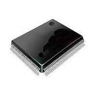
ST92F120V1Q7 STMicroelectronics, ST92F120V1Q7 Datasheet - Page 9

ST92F120V1Q7
Manufacturer Part Number
ST92F120V1Q7
Description
Microcontrollers (MCU) Flash 128K SPI/I2C
Manufacturer
STMicroelectronics
Datasheet
1.ST92F120V9Q7.pdf
(325 pages)
Specifications of ST92F120V1Q7
Data Bus Width
8 bit, 16 bit
Program Memory Type
Flash
Program Memory Size
128 KB
Data Ram Size
4 KB
Interface Type
I2C, SPI
Maximum Clock Frequency
24 MHz
Number Of Programmable I/os
77
Number Of Timers
5
Maximum Operating Temperature
+ 105 C
Mounting Style
SMD/SMT
Package / Case
PQFP-100
Minimum Operating Temperature
- 40 C
On-chip Adc
8 bit, 16 Channel
Lead Free Status / Rohs Status
No
Available stocks
Company
Part Number
Manufacturer
Quantity
Price
Company:
Part Number:
ST92F120V1Q7
Manufacturer:
ST
Quantity:
6 765
Part Number:
ST92F120V1Q7
Manufacturer:
ST
Quantity:
20 000
Part Number:
ST92F120V1Q7C
Manufacturer:
ST
Quantity:
20 000
Company:
Part Number:
ST92F120V1Q7DTR
Manufacturer:
MAXIM
Quantity:
2 854
- Current page: 9 of 325
- Download datasheet (3Mb)
1.2.4.3 Internal Circuitry: Digital I/O pin
In
pin able to operate either as an input or as an out-
put is shown. The circuitry implements a standard
input buffer and a push-pull configuration for the
output buffer. It is evident that although it is possi-
ble to disable the output buffer when the input sec-
tion is used, the MOS transistors of the buffer itself
can still affect the behaviour of the pin when ex-
posed to illegal conditions. In fact, the P-channel
transistor of the output buffer implements a direct
diode to V
the pin and N-well connected to V
channel of the output buffer implements a diode to
V
sion of the drain connected to the pin). In parallel
to these diodes, dedicated circuitry is implemented
to protect the logic from ESD events (MOS, diodes
and input series resistor).
The most important characteristic of these extra
devices is that they must not disturb normal oper-
ating modes, while acting during exposure to over
Figure 4. Digital Input/Output - True Open Drain Output
SS
Figure 3
(P-substrate connected to VSS and N-diffu-
DD
a schematic representation of an ST9
(P-diffusion of the drain connected to
P IN
ESD PROTECTION
DD
CIRCUITRY
), while the N-
N
I/O CIRCUITRY
limit conditions, avoiding permanent damage to
the logic circuitry.
All I/O pins can generally be programmed to work
also as open-drain outputs, by simply writing in the
corresponding register of the I/O Port. The gate of
the P-channel of the output buffer is disabled: it is
important to highlight that physically the P-channel
transistor is still present, so the diode to V
works. In some applications it can occur that the
voltage applied to the pin is higher than the V
value (supposing the external line is kept high,
while the ST9 power supply is turned off): this con-
dition will inject current through the diode, risking
permanent damages to the device.
In any case, programming I/O pins as open-drain
can help when several pins in the system are tied
to the same point: of course software must pay at-
tention to program only one of them as output at
any time, to avoid output driver contentions; it is
advisable to configure these pins as output open-
drain in order to reduce the risk of current conten-
tions.
O U TP U T
B U FFE R
PORT CIRCUITRY
ST92F120 - GENERAL DESCRIPTION
E N
P
N
N
E N
B U FFE R
IN P U T
P
9/324
1
DD
DD
Related parts for ST92F120V1Q7
Image
Part Number
Description
Manufacturer
Datasheet
Request
R

Part Number:
Description:
8/16-bit Flash Mcu Family With Ram, Eeprom And J1850 Blpd
Manufacturer:
STMicroelectronics
Datasheet:

Part Number:
Description:
STMicroelectronics [RIPPLE-CARRY BINARY COUNTER/DIVIDERS]
Manufacturer:
STMicroelectronics
Datasheet:

Part Number:
Description:
STMicroelectronics [LIQUID-CRYSTAL DISPLAY DRIVERS]
Manufacturer:
STMicroelectronics
Datasheet:

Part Number:
Description:
BOARD EVAL FOR MEMS SENSORS
Manufacturer:
STMicroelectronics
Datasheet:

Part Number:
Description:
NPN TRANSISTOR POWER MODULE
Manufacturer:
STMicroelectronics
Datasheet:

Part Number:
Description:
TURBOSWITCH ULTRA-FAST HIGH VOLTAGE DIODE
Manufacturer:
STMicroelectronics
Datasheet:

Part Number:
Description:
Manufacturer:
STMicroelectronics
Datasheet:

Part Number:
Description:
DIODE / SCR MODULE
Manufacturer:
STMicroelectronics
Datasheet:

Part Number:
Description:
DIODE / SCR MODULE
Manufacturer:
STMicroelectronics
Datasheet:

Part Number:
Description:
Search -----> STE16N100
Manufacturer:
STMicroelectronics
Datasheet:

Part Number:
Description:
Search ---> STE53NA50
Manufacturer:
STMicroelectronics
Datasheet:

Part Number:
Description:
NPN Transistor Power Module
Manufacturer:
STMicroelectronics
Datasheet:


