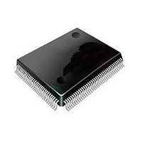
ST92F120V1Q7 STMicroelectronics, ST92F120V1Q7 Datasheet - Page 107

ST92F120V1Q7
Manufacturer Part Number
ST92F120V1Q7
Description
Microcontrollers (MCU) Flash 128K SPI/I2C
Manufacturer
STMicroelectronics
Datasheet
1.ST92F120V9Q7.pdf
(325 pages)
Specifications of ST92F120V1Q7
Data Bus Width
8 bit, 16 bit
Program Memory Type
Flash
Program Memory Size
128 KB
Data Ram Size
4 KB
Interface Type
I2C, SPI
Maximum Clock Frequency
24 MHz
Number Of Programmable I/os
77
Number Of Timers
5
Maximum Operating Temperature
+ 105 C
Mounting Style
SMD/SMT
Package / Case
PQFP-100
Minimum Operating Temperature
- 40 C
On-chip Adc
8 bit, 16 Channel
Lead Free Status / Rohs Status
No
Available stocks
Company
Part Number
Manufacturer
Quantity
Price
Company:
Part Number:
ST92F120V1Q7
Manufacturer:
ST
Quantity:
6 765
Part Number:
ST92F120V1Q7
Manufacturer:
ST
Quantity:
20 000
Part Number:
ST92F120V1Q7C
Manufacturer:
ST
Quantity:
20 000
Company:
Part Number:
ST92F120V1Q7DTR
Manufacturer:
MAXIM
Quantity:
2 854
- Current page: 107 of 325
- Download datasheet (3Mb)
RESET/STOP MANAGER (Cont’d)
The on-chip Timer/Watchdog generates a reset
condition if the Watchdog mode is enabled
(WCR.WDGEN cleared, R252 page 0), and if the
programmed period elapses without the specific
code (AAh, 55h) written to the appropriate register.
The input pin RESET is not driven low by the on-
chip reset generated by the Timer/Watchdog.
When the Reset pin goes high again, a deterministic
number of oscillator clock cycles (CLOCK1) is
counted (refer to T
state ( 1 CLOCK1 period, depending on the delay
between the rising edge of the Reset pin and the first
rising edge of CLOCK1). Subsequently a short Boot
routine is executed from the device internal Boot
memory, and control then passes to the user pro-
gram.
The Boot routine sets the device characteristics
and loads the correct values in the Memory Man-
agement Unit’s pointer registers, so that these
point to the physical memory areas as mapped in
the specific device. The precise duration of this
short Boot routine varies from device to device,
depending on the Boot memory contents.
At the end of the Boot routine the Program Coun-
ter will be set to the location specified in the Reset
Vector located in the lowest two bytes of memory.
7.6.1 Reset Pin Timing
To improve the noise immunity of the device, the
Reset pin has a Schmitt trigger input circuit with
hysteresis. In addition, a filter will prevent an un-
wanted reset in case of a single glitch of less than
Figure 55. Reset Pin Input Structure
RSPH
P IN
) before exiting the Reset
ESD PROTECTION
CIRCUITRY
ST92F120 - RESET AND CLOCK CONTROL UNIT (RCCU)
TO GENERATE RESET SIGNAL
SCHMITT TRIGGER and LOW
50 ns on the Reset pin. The device is certain to re-
set if a negative pulse of more than 20 s is ap-
plied. When the reset pin goes high again, a delay
of up to 4 s will elapse before the RCCU detects
this rising front. From this event on, a defined
number of CLOCK1 cycles (refer to T
counted
( 1CLOCK1 period depending on the delay be-
tween the positive edge the RCCU detects and the
first rising edge of CLOCK1)
If the ST9 is a ROMLESS version, without on-chip
program memory, the memory interface ports are
set to external memory mode (i.e Alternate Func-
tion) and the memory accesses are made to exter-
nal Program memory with wait cycles insertion.
Figure 54. Recommended Signal to be Applied
on Reset Pin
V
V
V
RESETN
IHRS
ILRS
V
DD
PASS FILTER
before
exiting
Minimum
20 s
the
Reset
RSPH
107/324
state
) is
9
Related parts for ST92F120V1Q7
Image
Part Number
Description
Manufacturer
Datasheet
Request
R

Part Number:
Description:
8/16-bit Flash Mcu Family With Ram, Eeprom And J1850 Blpd
Manufacturer:
STMicroelectronics
Datasheet:

Part Number:
Description:
STMicroelectronics [RIPPLE-CARRY BINARY COUNTER/DIVIDERS]
Manufacturer:
STMicroelectronics
Datasheet:

Part Number:
Description:
STMicroelectronics [LIQUID-CRYSTAL DISPLAY DRIVERS]
Manufacturer:
STMicroelectronics
Datasheet:

Part Number:
Description:
BOARD EVAL FOR MEMS SENSORS
Manufacturer:
STMicroelectronics
Datasheet:

Part Number:
Description:
NPN TRANSISTOR POWER MODULE
Manufacturer:
STMicroelectronics
Datasheet:

Part Number:
Description:
TURBOSWITCH ULTRA-FAST HIGH VOLTAGE DIODE
Manufacturer:
STMicroelectronics
Datasheet:

Part Number:
Description:
Manufacturer:
STMicroelectronics
Datasheet:

Part Number:
Description:
DIODE / SCR MODULE
Manufacturer:
STMicroelectronics
Datasheet:

Part Number:
Description:
DIODE / SCR MODULE
Manufacturer:
STMicroelectronics
Datasheet:

Part Number:
Description:
Search -----> STE16N100
Manufacturer:
STMicroelectronics
Datasheet:

Part Number:
Description:
Search ---> STE53NA50
Manufacturer:
STMicroelectronics
Datasheet:

Part Number:
Description:
NPN Transistor Power Module
Manufacturer:
STMicroelectronics
Datasheet:


