DK-DEV-1AGX60N Altera, DK-DEV-1AGX60N Datasheet - Page 92
DK-DEV-1AGX60N
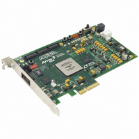
Manufacturer Part Number
DK-DEV-1AGX60N
Description
KIT DEV ARRIA GX 1AGX60N
Manufacturer
Altera
Series
Arria GXr
Type
FPGAr
Datasheet
1.EP1AGX20CF484C6N.pdf
(234 pages)
Specifications of DK-DEV-1AGX60N
Contents
Dev. Board, Quartus® II Web Edition, Reference Designs, Labs, and Complete Documentation
For Use With/related Products
1AGX60N
Lead Free Status / RoHS Status
Lead free / RoHS Compliant
Other names
544-2372
Available stocks
Company
Part Number
Manufacturer
Quantity
Price


2–86
Figure 2–72. Arria GX IOE in Bidirectional I/O Configuration
Notes to
(1) All input signals to the IOE can be inverted at the IOE.
(2) The optional PCI clamp is only available on column I/O pins.
Arria GX Device Handbook, Volume 1
Column, Row,
Interconnect
Figure
or Local
2–72:
ioe_clk[7..0]
In normal bidirectional operation, you can use the input register for input data
requiring fast setup times. The input register can have its own clock input and clock
enable separate from the OE and output registers. The output register can be used for
data requiring fast clock-to-output performance. You can use the OE register for fast
clock-to-output enable timing. The OE and output register share the same clock
source and the same clock enable source from the local interconnect in the associated
LAB, dedicated I/O clocks, and the column and row interconnects.
the IOE in bidirectional configuration.
The Arria GX device IOE includes programmable delays that can be activated to
ensure input IOE register-to-logic array register transfers, input pin-to-logic array
register transfers, or output IOE register-to-pin transfers.
clkout
clkin
oe
ce_out
aclr/apreset
ce_in
sclr/spreset
Chip-Wide Reset
Output Register
OE Register
Input Register
D
CLRN/PRN
ENA
ENA
D
ENA
CLRN/PRN
D
CLRN/PRN
(Note 1)
Q
Q
Q
Drive Strength Control
Open-Drain Output
Pin Delay
Output
Input Register Delay
Logic Array Delay
Input Pin to
Input Pin to
OE Register
t
CO
Delay
V
CCIO
© December 2009 Altera Corporation
Chapter 2: Arria GX Architecture
PCI Clamp (2)
V
CCIO
Bus-Hold
Termination
Circuit
Figure 2–72
On-Chip
Programmable
Pull-Up
Resistor
I/O Structure
shows
Related parts for DK-DEV-1AGX60N
Image
Part Number
Description
Manufacturer
Datasheet
Request
R

Part Number:
Description:
KIT DEV ARRIA II GX FPGA 2AGX125
Manufacturer:
Altera
Datasheet:

Part Number:
Description:
KIT DEV CYCLONE III LS EP3CLS200
Manufacturer:
Altera
Datasheet:

Part Number:
Description:
KIT DEV STRATIX IV FPGA 4SE530
Manufacturer:
Altera
Datasheet:

Part Number:
Description:
KIT DEV FPGA 2AGX260 W/6.375G TX
Manufacturer:
Altera
Datasheet:

Part Number:
Description:
KIT DEV MAX V 5M570Z
Manufacturer:
Altera
Datasheet:

Part Number:
Description:
KIT DEV STRATIX V FPGA 5SGXEA7
Manufacturer:
Altera
Datasheet:

Part Number:
Description:
KIT DEVELOPMENT STRATIX III
Manufacturer:
Altera
Datasheet:

Part Number:
Description:
KIT DEVELOPMENT STRATIX IV
Manufacturer:
Altera
Datasheet:
Part Number:
Description:
KIT STARTER CYCLONE IV GX
Manufacturer:
Altera
Datasheet:
Part Number:
Description:
KIT DEVELOPMENT STRATIX IV
Manufacturer:
Altera
Datasheet:

Part Number:
Description:
CPLD, EP610 Family, ECMOS Process, 300 Gates, 16 Macro Cells, 16 Reg., 16 User I/Os, 5V Supply, 35 Speed Grade, 24DIP
Manufacturer:
Altera Corporation
Datasheet:
Part Number:
Description:
CPLD, EP610 Family, ECMOS Process, 300 Gates, 16 Macro Cells, 16 Reg., 16 User I/Os, 5V Supply, 15 Speed Grade, 24DIP
Manufacturer:
Altera Corporation
Datasheet: