DK-DEV-1AGX60N Altera, DK-DEV-1AGX60N Datasheet - Page 11
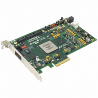
DK-DEV-1AGX60N
Manufacturer Part Number
DK-DEV-1AGX60N
Description
KIT DEV ARRIA GX 1AGX60N
Manufacturer
Altera
Series
Arria GXr
Type
FPGAr
Datasheet
1.EP1AGX20CF484C6N.pdf
(234 pages)
Specifications of DK-DEV-1AGX60N
Contents
Dev. Board, Quartus® II Web Edition, Reference Designs, Labs, and Complete Documentation
For Use With/related Products
1AGX60N
Lead Free Status / RoHS Status
Lead free / RoHS Compliant
Other names
544-2372
Available stocks
Company
Part Number
Manufacturer
Quantity
Price


Chapter 2: Arria GX Architecture
Transceivers
© December 2009 Altera Corporation
f
1
■
Altera
REFCLK1) to provide reference clock for the transmitter PLL.
Table 2–2
Table 2–2. Transmitter PLL Specifications
The transmitter PLL output feeds the central clock divider block and the local clock
divider blocks. These clock divider blocks divide the high-speed serial clock to
generate the low-speed parallel clock for the transceiver PCS logic and
PLD-transceiver interface clock.
Transmitter Phase Compensation FIFO Buffer
A transmitter phase compensation FIFO is located at each transmitter channel’s logic
array interface. It compensates for the phase difference between the transmitter PCS
clock and the local PLD clock. The transmitter phase compensation FIFO is used in all
supported functional modes. The transmitter phase compensation FIFO buffer is eight
words deep in PCI Express (PIPE) mode and four words deep in all other modes.
For more information about architecture and clocking, refer to the
Architecture
Byte Serializer
The byte serializer takes in two-byte wide data from the transmitter phase
compensation FIFO buffer and serializes it into a one-byte wide data at twice the
speed. The transmit data path after the byte serializer is 8 or 10 bits. This allows
clocking the PLD-transceiver interface at half the speed when compared with the
transmitter PCS logic. The byte serializer is bypassed in GIGE mode. After
serialization, the byte serializer transmits the least significant byte (LSByte) first and
the most significant byte (MSByte) last.
Input reference frequency range
Data rate support
Bandwidth
Inter-transceiver block lines driven by reference clock input pins of other
transceiver blocks
®
recommends using the dedicated reference clock input pins (REFCLK0 or
lists the adjustable parameters in the transmitter PLL.
chapter.
Parameter
600 Mbps to 3.125 Gbps
50 MHz to 622.08 MHz
Low, medium, or high
Specifications
Arria GX Device Handbook, Volume 1
Arria GX Transceiver
2–5
Related parts for DK-DEV-1AGX60N
Image
Part Number
Description
Manufacturer
Datasheet
Request
R

Part Number:
Description:
KIT DEV ARRIA II GX FPGA 2AGX125
Manufacturer:
Altera
Datasheet:

Part Number:
Description:
KIT DEV CYCLONE III LS EP3CLS200
Manufacturer:
Altera
Datasheet:

Part Number:
Description:
KIT DEV STRATIX IV FPGA 4SE530
Manufacturer:
Altera
Datasheet:

Part Number:
Description:
KIT DEV FPGA 2AGX260 W/6.375G TX
Manufacturer:
Altera
Datasheet:

Part Number:
Description:
KIT DEV MAX V 5M570Z
Manufacturer:
Altera
Datasheet:

Part Number:
Description:
KIT DEV STRATIX V FPGA 5SGXEA7
Manufacturer:
Altera
Datasheet:

Part Number:
Description:
KIT DEVELOPMENT STRATIX III
Manufacturer:
Altera
Datasheet:

Part Number:
Description:
KIT DEVELOPMENT STRATIX IV
Manufacturer:
Altera
Datasheet:
Part Number:
Description:
KIT STARTER CYCLONE IV GX
Manufacturer:
Altera
Datasheet:
Part Number:
Description:
KIT DEVELOPMENT STRATIX IV
Manufacturer:
Altera
Datasheet:

Part Number:
Description:
CPLD, EP610 Family, ECMOS Process, 300 Gates, 16 Macro Cells, 16 Reg., 16 User I/Os, 5V Supply, 35 Speed Grade, 24DIP
Manufacturer:
Altera Corporation
Datasheet:
Part Number:
Description:
CPLD, EP610 Family, ECMOS Process, 300 Gates, 16 Macro Cells, 16 Reg., 16 User I/Os, 5V Supply, 15 Speed Grade, 24DIP
Manufacturer:
Altera Corporation
Datasheet: