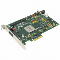
DK-DEV-1AGX60N Altera, DK-DEV-1AGX60N Datasheet - Page 137

DK-DEV-1AGX60N
Manufacturer Part Number
DK-DEV-1AGX60N
Description
KIT DEV ARRIA GX 1AGX60N
Manufacturer
Altera
Series
Arria GXr
Type
FPGAr
Datasheet
1.EP1AGX20CF484C6N.pdf
(234 pages)
Specifications of DK-DEV-1AGX60N
Contents
Dev. Board, Quartus® II Web Edition, Reference Designs, Labs, and Complete Documentation
For Use With/related Products
1AGX60N
Lead Free Status / RoHS Status
Lead free / RoHS Compliant
Other names
544-2372
Available stocks
Company
Part Number
Manufacturer
Quantity
Price
- Current page: 137 of 234
- Download datasheet (4Mb)
Chapter 4: DC and Switching Characteristics
Operating Conditions
Table 4–14. Arria GX Device DC Operating Conditions (Part 2 of 2)
I/O Standard Specifications
Table 4–15. LVTTL Specifications
Table 4–16. LVCMOS Specifications
© December 2009 Altera Corporation
R
Notes to
(1) Typical values are for T
(2) This value is specified for normal device operation. The value may vary during power-up. This applies for all V
(3) Maximum values depend on the actual TJ and design utilization. For maximum values, refer to the Excel-based PowerPlay Early Power Estimator
(4) Pin pull-up resistance values will be lower if an external source drives the pin higher than V
V
V
V
V
V
Notes to
(1) Arria GX devices comply to the narrow range for the supply voltage as specified in the EIA/JEDEC Standard, JESD8-B.
(2) This specification is supported across all the programmable drive strength settings available for this I/O standard.
V
V
V
V
V
Notes to
(1) Arria GX devices comply to the narrow range for the supply voltage as specified in the EIA/JEDEC Standard, JESD8-B.
(2) This specification is supported across all the programmable drive strength available for this I/O standard.
CCIO
IH
IL
OH
OL
CCIO
IH
IL
OH
OL
CONF
Symbol
and 1.2 V).
(available at
values. For more information, refer to
Symbol
Symbol
(1)
(1)
(4)
Table
Table
Table
4–14:
4–15:
4–16:
Value of I/O pin pull-up
resistor before and during
configuration
Recommended value of
I/O pin external pull-down
resistor before and during
configuration
PowerPlay Early Power Estimators (EPE) and Power
Output supply voltage
High-level input voltage
Low-level input voltage
High-level output voltage
Low-level output voltage
Output supply voltage
High-level input voltage
Low-level input voltage
High-level output voltage
Low-level output voltage
Parameter
Table 4–15
specifications.
A
= 25 °C, V
Parameter
Parameter
CCINT
through
“Power Consumption” on page
= 1.2 V, and V
V
V
V
V
V
i
i
i
i
i
= 0, V
= 0, V
= 0, V
= 0, V
= 0, V
Table 4–38
I
I
OH
OL
CCIO
= 4 mA
= –4 mA
V
V
Conditions
CCIO
CCIO
CCIO
CCIO
CCIO
CCIO
CCIO
= 1.2 V, 1.5 V, 1.8 V, 2.5 V, and 3.3 V.
Conditions
= 3.3 V
= 2.5 V
= 1.8 V
= 1.5 V
= 1.2 V
—
= 3.0, I
= 3.0, I
(2)
—
—
—
Analyzer) or the Quartus
(2)
show the Arria GX device family I/O standard
Conditions
OH
OL
4–25.
—
—
—
= 0.1 mA
= –0.1 mA
(Note 1)
(2)
Device
(2)
—
—
—
—
—
—
®
Minimum
CCIO
II PowerPlay Power Analyzer feature for maximum
3.135
–0.3
1.7
2.4
—
.
V
Minimum
CCIO
3.135
–0.3
1.7
—
– 0.2
Min
10
15
30
40
50
—
Arria GX Device Handbook, Volume 1
CCIO
Maximum
Typ
25
35
50
75
90
settings (3.3, 2.5, 1.8, 1.5,
1
3.465
Maximum
0.45
4.0
0.8
—
3.465
4.0
0.8
0.2
—
Max
100
150
170
50
70
2
Units
Units
Units
V
V
V
V
V
V
V
V
V
V
k
k
k
k
k
k
4–15
Related parts for DK-DEV-1AGX60N
Image
Part Number
Description
Manufacturer
Datasheet
Request
R

Part Number:
Description:
KIT DEV ARRIA II GX FPGA 2AGX125
Manufacturer:
Altera
Datasheet:

Part Number:
Description:
KIT DEV CYCLONE III LS EP3CLS200
Manufacturer:
Altera
Datasheet:

Part Number:
Description:
KIT DEV STRATIX IV FPGA 4SE530
Manufacturer:
Altera
Datasheet:

Part Number:
Description:
KIT DEV FPGA 2AGX260 W/6.375G TX
Manufacturer:
Altera
Datasheet:

Part Number:
Description:
KIT DEV MAX V 5M570Z
Manufacturer:
Altera
Datasheet:

Part Number:
Description:
KIT DEV STRATIX V FPGA 5SGXEA7
Manufacturer:
Altera
Datasheet:

Part Number:
Description:
KIT DEVELOPMENT STRATIX III
Manufacturer:
Altera
Datasheet:

Part Number:
Description:
KIT DEVELOPMENT STRATIX IV
Manufacturer:
Altera
Datasheet:

Part Number:
Description:
KIT STARTER CYCLONE IV GX
Manufacturer:
Altera
Datasheet:

Part Number:
Description:
KIT DEVELOPMENT STRATIX IV
Manufacturer:
Altera
Datasheet:

Part Number:
Description:
CPLD, EP610 Family, ECMOS Process, 300 Gates, 16 Macro Cells, 16 Reg., 16 User I/Os, 5V Supply, 35 Speed Grade, 24DIP
Manufacturer:
Altera Corporation
Datasheet:

Part Number:
Description:
CPLD, EP610 Family, ECMOS Process, 300 Gates, 16 Macro Cells, 16 Reg., 16 User I/Os, 5V Supply, 15 Speed Grade, 24DIP
Manufacturer:
Altera Corporation
Datasheet:


