DK-DEV-1AGX60N Altera, DK-DEV-1AGX60N Datasheet - Page 30
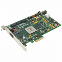
DK-DEV-1AGX60N
Manufacturer Part Number
DK-DEV-1AGX60N
Description
KIT DEV ARRIA GX 1AGX60N
Manufacturer
Altera
Series
Arria GXr
Type
FPGAr
Datasheet
1.EP1AGX20CF484C6N.pdf
(234 pages)
Specifications of DK-DEV-1AGX60N
Contents
Dev. Board, Quartus® II Web Edition, Reference Designs, Labs, and Complete Documentation
For Use With/related Products
1AGX60N
Lead Free Status / RoHS Status
Lead free / RoHS Compliant
Other names
544-2372
Available stocks
Company
Part Number
Manufacturer
Quantity
Price


2–24
Table 2–6. Reset Signal Map to Arria GX Blocks
Calibration Block
Transceiver Clocking
Arria GX Device Handbook, Volume 1
rx_digitalreset
rx_analogreset
tx_digitalreset
gxb_powerdown
gxb_enable
Reset Signal
Table 2–6
circuitry affected by each signal.
Arria GX devices use the calibration block to calibrate OCT for the PLLs, and their
associated output buffers, and the terminating resistors on the transceivers. The
calibration block counters the effects of process, voltage, and temperature (PVT). The
calibration block references a derived voltage across an external reference resistor to
calibrate the OCT resistors on Arria GX devices. You can power down the calibration
block. However, powering down the calibration block during operations can yield
transmit and receive data errors.
This section describes the clock distribution in an Arria GX transceiver channel and
the PLD clock resource utilization by the transceiver blocks.
Transceiver Channel Clock Distribution
Each transceiver block has one transmitter PLL and four receiver PLLs.
—
—
v
v
v
—
—
v
v
v
lists the reset signals available in Arria GX devices and the transceiver
v
v
—
—
—
—
—
—
v
v
v
v
—
—
—
—
—
v
v
v
—
—
v
v
v
v
v
v
—
—
v
v
v
—
—
—
—
—
—
—
v
—
—
v
v
v
v
v
—
—
© December 2009 Altera Corporation
Chapter 2: Arria GX Architecture
v
—
—
v
v
v
v
v
—
—
v
—
—
v
v
Transceivers
v
v
v
—
—
v
v
v
—
—
Related parts for DK-DEV-1AGX60N
Image
Part Number
Description
Manufacturer
Datasheet
Request
R

Part Number:
Description:
KIT DEV ARRIA II GX FPGA 2AGX125
Manufacturer:
Altera
Datasheet:

Part Number:
Description:
KIT DEV CYCLONE III LS EP3CLS200
Manufacturer:
Altera
Datasheet:

Part Number:
Description:
KIT DEV STRATIX IV FPGA 4SE530
Manufacturer:
Altera
Datasheet:

Part Number:
Description:
KIT DEV FPGA 2AGX260 W/6.375G TX
Manufacturer:
Altera
Datasheet:

Part Number:
Description:
KIT DEV MAX V 5M570Z
Manufacturer:
Altera
Datasheet:

Part Number:
Description:
KIT DEV STRATIX V FPGA 5SGXEA7
Manufacturer:
Altera
Datasheet:

Part Number:
Description:
KIT DEVELOPMENT STRATIX III
Manufacturer:
Altera
Datasheet:

Part Number:
Description:
KIT DEVELOPMENT STRATIX IV
Manufacturer:
Altera
Datasheet:
Part Number:
Description:
KIT STARTER CYCLONE IV GX
Manufacturer:
Altera
Datasheet:
Part Number:
Description:
KIT DEVELOPMENT STRATIX IV
Manufacturer:
Altera
Datasheet:

Part Number:
Description:
CPLD, EP610 Family, ECMOS Process, 300 Gates, 16 Macro Cells, 16 Reg., 16 User I/Os, 5V Supply, 35 Speed Grade, 24DIP
Manufacturer:
Altera Corporation
Datasheet:
Part Number:
Description:
CPLD, EP610 Family, ECMOS Process, 300 Gates, 16 Macro Cells, 16 Reg., 16 User I/Os, 5V Supply, 15 Speed Grade, 24DIP
Manufacturer:
Altera Corporation
Datasheet: