DK-DEV-1AGX60N Altera, DK-DEV-1AGX60N Datasheet - Page 226
DK-DEV-1AGX60N
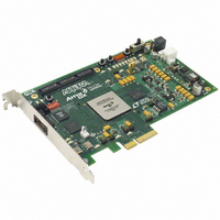
Manufacturer Part Number
DK-DEV-1AGX60N
Description
KIT DEV ARRIA GX 1AGX60N
Manufacturer
Altera
Series
Arria GXr
Type
FPGAr
Datasheet
1.EP1AGX20CF484C6N.pdf
(234 pages)
Specifications of DK-DEV-1AGX60N
Contents
Dev. Board, Quartus® II Web Edition, Reference Designs, Labs, and Complete Documentation
For Use With/related Products
1AGX60N
Lead Free Status / RoHS Status
Lead free / RoHS Compliant
Other names
544-2372
Available stocks
Company
Part Number
Manufacturer
Quantity
Price


4–104
Table 4–116. Enhanced PLL Specifications (Part 2 of 2)
Table 4–117. Fast PLL Specifications (Part 1 of 2)
Arria GX Device Handbook, Volume 1
t
Notes to
(1) This is limited by the I/O f
(2) If the counter cascading feature of the PLL is used, there is no minimum output clock frequency.
f
f
f
t
f
f
f
t
f
t
t
t
RECONFIGWAIT
IN
INPFD
INDUTY
INJITTER
VCO
OUT
OUT_EXT
CONFIGPLL
CLBW
LOCK
PLL_PSERR
ARESET
Name
Table
Name
4–116:
The time required for the wait after the
reconfiguration is done and the areset is
applied.
Input clock frequency
Input frequency to the
PFD
Input clock duty cycle
Input clock jitter
tolerance in terms of
period jitter.
Bandwidth
Input clock jitter
tolerance in terms of
period jitter.
Bandwidth 0.2 MHz
Upper VCO frequency
range
Lower VCO frequency
range
PLL output frequency
to
PLL output frequency
to LVDS or DPA clock
PLL clock output
frequency to regular
I/O
Time required to
reconfigure scan
chains for fast PLLs
PLL closed-loop
bandwidth
Time required for the
PLL to lock from the
time it is enabled or
the end of the device
configuration
Accuracy of PLL phase
shift
Minimum pulse width
on
MAX
GCLK
areset
.
Description
or
RCLK
signal.
2 MHz
Description
4.6875
4.6875
16.08
16.08
1.16
Min
300
150
150
40
—
—
—
—
—
10
75/f
0.03
Typ
0.5
1.0
—
—
—
—
—
—
—
—
SCANCLK
—
—
5
Min
—
Chapter 4: DC and Switching Characteristics
Max
640
500
840
420
550
840
±30
Typ
—
(1)
60
—
—
—
28
—
1
© December 2009 Altera Corporation
Max
2
PLL Timing Specifications
ns (p-p)
ns (p-p)
Units
MHz
MHz
MHz
MHz
MHz
MHz
MHz
MHz
ms
ns
ps
ns
%
Units
us
Related parts for DK-DEV-1AGX60N
Image
Part Number
Description
Manufacturer
Datasheet
Request
R

Part Number:
Description:
KIT DEV ARRIA II GX FPGA 2AGX125
Manufacturer:
Altera
Datasheet:

Part Number:
Description:
KIT DEV CYCLONE III LS EP3CLS200
Manufacturer:
Altera
Datasheet:

Part Number:
Description:
KIT DEV STRATIX IV FPGA 4SE530
Manufacturer:
Altera
Datasheet:

Part Number:
Description:
KIT DEV FPGA 2AGX260 W/6.375G TX
Manufacturer:
Altera
Datasheet:

Part Number:
Description:
KIT DEV MAX V 5M570Z
Manufacturer:
Altera
Datasheet:

Part Number:
Description:
KIT DEV STRATIX V FPGA 5SGXEA7
Manufacturer:
Altera
Datasheet:

Part Number:
Description:
KIT DEVELOPMENT STRATIX III
Manufacturer:
Altera
Datasheet:

Part Number:
Description:
KIT DEVELOPMENT STRATIX IV
Manufacturer:
Altera
Datasheet:
Part Number:
Description:
KIT STARTER CYCLONE IV GX
Manufacturer:
Altera
Datasheet:
Part Number:
Description:
KIT DEVELOPMENT STRATIX IV
Manufacturer:
Altera
Datasheet:

Part Number:
Description:
CPLD, EP610 Family, ECMOS Process, 300 Gates, 16 Macro Cells, 16 Reg., 16 User I/Os, 5V Supply, 35 Speed Grade, 24DIP
Manufacturer:
Altera Corporation
Datasheet:
Part Number:
Description:
CPLD, EP610 Family, ECMOS Process, 300 Gates, 16 Macro Cells, 16 Reg., 16 User I/Os, 5V Supply, 15 Speed Grade, 24DIP
Manufacturer:
Altera Corporation
Datasheet: