DK-DEV-1AGX60N Altera, DK-DEV-1AGX60N Datasheet - Page 24
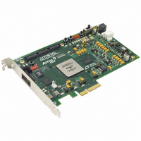
DK-DEV-1AGX60N
Manufacturer Part Number
DK-DEV-1AGX60N
Description
KIT DEV ARRIA GX 1AGX60N
Manufacturer
Altera
Series
Arria GXr
Type
FPGAr
Datasheet
1.EP1AGX20CF484C6N.pdf
(234 pages)
Specifications of DK-DEV-1AGX60N
Contents
Dev. Board, Quartus® II Web Edition, Reference Designs, Labs, and Complete Documentation
For Use With/related Products
1AGX60N
Lead Free Status / RoHS Status
Lead free / RoHS Compliant
Other names
544-2372
Available stocks
Company
Part Number
Manufacturer
Quantity
Price


2–18
Arria GX Device Handbook, Volume 1
1
XAUI Mode
In XAUI mode, the rate matcher adheres to clause 48 of the IEEE 802.3ae specification
for clock rate compensation. The rate matcher performs clock compensation on
columns of /R/ (/K28.0/), denoted by //R//. An //R// is added or deleted
automatically based on the number of words in the FIFO buffer.
PCI Express (PIPE) Mode Rate Matcher
In PCI Express (PIPE) mode, the rate matcher can compensate up to ± 300 PPM
(600 PPM total) frequency difference between the upstream transmitter and the
receiver. The rate matcher logic looks for skip ordered sets (SOS), which contains a
/K28.5/ comma followed by three /K28.0/ skip characters. The rate matcher logic
deletes or inserts /K28.0/ skip characters as necessary from/to the rate matcher FIFO.
The rate matcher in PCI Express (PIPE) mode has a FIFO buffer overflow and
underflow protection. In the event of a FIFO buffer overflow, the rate matcher deletes
any data after detecting the overflow condition to prevent FIFO pointer corruption
until the rate matcher is not full. In an underflow condition, the rate matcher inserts
9'h1FE (/K30.7/) until the FIFO buffer is not empty. These measures ensure that the
FIFO buffer can gracefully exit the overflow and underflow condition without
requiring a FIFO reset. The rate matcher FIFO overflow and underflow condition is
indicated on the pipestatus port.
You can bypass the rate matcher in PCI Express (PIPE) mode if you have a
synchronous system where the upstream transmitter and local receiver derive their
reference clocks from the same source.
GIGE Mode Rate Matcher
In GIGE mode, the rate matcher can compensate up to ± 100 PPM (200 PPM total)
frequency difference between the upstream transmitter and the receiver. The rate
matcher logic inserts or deletes /I2/ idle ordered sets to/from the rate matcher FIFO
during the inter-frame or inter-packet gap (IFG or IPG). /I2/ is selected as the rate
matching ordered set because it maintains the running disparity, unlike /I1/ that
alters the running disparity. Because the /I2/ ordered-set contains two 10-bit code
groups (/K28.5/, /D16.2/), 20 bits are inserted or deleted at a time for rate matching.
The rate matcher logic has the capability to insert or delete /C1/ or /C2/
configuration ordered sets when ‘GIGE Enhanced’ mode is chosen as the sub-protocol
in the MegaWizard Plug-In Manager.
If the frequency PPM difference between the upstream transmitter and the local
receiver is high, or if the packet size is too large, the rate matcher FIFO buffer can face
an overflow or underflow situation.
Basic Mode
In basic mode, you can program the skip and control pattern for rate matching. There
is no restriction on the deletion of a skip character in a cluster. The rate matcher
deletes the skip characters as long as they are available. For insertion, the rate matcher
inserts skip characters such that the number of skip characters at the output of rate
matcher does not exceed five.
© December 2009 Altera Corporation
Chapter 2: Arria GX Architecture
Transceivers
Related parts for DK-DEV-1AGX60N
Image
Part Number
Description
Manufacturer
Datasheet
Request
R

Part Number:
Description:
KIT DEV ARRIA II GX FPGA 2AGX125
Manufacturer:
Altera
Datasheet:

Part Number:
Description:
KIT DEV CYCLONE III LS EP3CLS200
Manufacturer:
Altera
Datasheet:

Part Number:
Description:
KIT DEV STRATIX IV FPGA 4SE530
Manufacturer:
Altera
Datasheet:

Part Number:
Description:
KIT DEV FPGA 2AGX260 W/6.375G TX
Manufacturer:
Altera
Datasheet:

Part Number:
Description:
KIT DEV MAX V 5M570Z
Manufacturer:
Altera
Datasheet:

Part Number:
Description:
KIT DEV STRATIX V FPGA 5SGXEA7
Manufacturer:
Altera
Datasheet:

Part Number:
Description:
KIT DEVELOPMENT STRATIX III
Manufacturer:
Altera
Datasheet:

Part Number:
Description:
KIT DEVELOPMENT STRATIX IV
Manufacturer:
Altera
Datasheet:
Part Number:
Description:
KIT STARTER CYCLONE IV GX
Manufacturer:
Altera
Datasheet:
Part Number:
Description:
KIT DEVELOPMENT STRATIX IV
Manufacturer:
Altera
Datasheet:

Part Number:
Description:
CPLD, EP610 Family, ECMOS Process, 300 Gates, 16 Macro Cells, 16 Reg., 16 User I/Os, 5V Supply, 35 Speed Grade, 24DIP
Manufacturer:
Altera Corporation
Datasheet:
Part Number:
Description:
CPLD, EP610 Family, ECMOS Process, 300 Gates, 16 Macro Cells, 16 Reg., 16 User I/Os, 5V Supply, 15 Speed Grade, 24DIP
Manufacturer:
Altera Corporation
Datasheet: