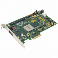
DK-DEV-1AGX60N Altera, DK-DEV-1AGX60N Datasheet - Page 56

DK-DEV-1AGX60N
Manufacturer Part Number
DK-DEV-1AGX60N
Description
KIT DEV ARRIA GX 1AGX60N
Manufacturer
Altera
Series
Arria GXr
Type
FPGAr
Datasheet
1.EP1AGX20CF484C6N.pdf
(234 pages)
Specifications of DK-DEV-1AGX60N
Contents
Dev. Board, Quartus® II Web Edition, Reference Designs, Labs, and Complete Documentation
For Use With/related Products
1AGX60N
Lead Free Status / RoHS Status
Lead free / RoHS Compliant
Other names
544-2372
Available stocks
Company
Part Number
Manufacturer
Quantity
Price
- Current page: 56 of 234
- Download datasheet (4Mb)
2–50
Figure 2–42. M512 RAM Block Control Signals
Arria GX Device Handbook, Volume 1
Dedicated
Row LAB
Clocks
Local
Interconnect
Local
Interconnect
Local
Interconnect
Local
Interconnect
Local
Interconnect
Local
Interconnect
Local
Interconnect
Local
Interconnect
When configured as RAM or ROM, you can use an initialization file to pre-load the
memory contents.
M512 RAM blocks can have different clocks on its inputs and outputs. The wren,
datain, and write address registers are all clocked together from one of the two
clocks feeding the block. The read address, rden, and output registers can be clocked
by either of the two clocks driving the block, allowing the RAM block to operate in
read and write or input and output clock modes. Only the output register can be
bypassed. The six labclk signals or local interconnect can drive the inclock,
outclock, wren, rden, and outclr signals. Because of the advanced interconnect
between the LAB and M512 RAM blocks, ALMs can also control the wren and rden
signals and the RAM clock, clock enable, and asynchronous clear signals.
shows the M512 RAM block control signal generation logic.
The RAM blocks in Arria GX devices have local interconnects to allow ALMs and
interconnects to drive into RAM blocks. The M512 RAM block local interconnect is
driven by the R4, C4, and direct link interconnects from adjacent LABs. The M512
RAM blocks can communicate with LABs on either the left or right side through these
row interconnects or with LAB columns on the left or right side with the column
interconnects. The M512 RAM block has up to 16 direct link input connections from
the left adjacent LABs and another 16 from the right adjacent LAB. M512 RAM
outputs can also connect to left and right LABs through direct link interconnect. The
M512 RAM block has equal opportunity for access and performance to and from
LABs on either its left or right side.
array interface.
6
inclock
inclocken
Figure 2–43
outclock
outclocken
shows the M512 RAM block to logic
rden
© December 2009 Altera Corporation
Chapter 2: Arria GX Architecture
wren
outclr
TriMatrix Memory
Figure 2–42
Related parts for DK-DEV-1AGX60N
Image
Part Number
Description
Manufacturer
Datasheet
Request
R

Part Number:
Description:
KIT DEV ARRIA II GX FPGA 2AGX125
Manufacturer:
Altera
Datasheet:

Part Number:
Description:
KIT DEV CYCLONE III LS EP3CLS200
Manufacturer:
Altera
Datasheet:

Part Number:
Description:
KIT DEV STRATIX IV FPGA 4SE530
Manufacturer:
Altera
Datasheet:

Part Number:
Description:
KIT DEV FPGA 2AGX260 W/6.375G TX
Manufacturer:
Altera
Datasheet:

Part Number:
Description:
KIT DEV MAX V 5M570Z
Manufacturer:
Altera
Datasheet:

Part Number:
Description:
KIT DEV STRATIX V FPGA 5SGXEA7
Manufacturer:
Altera
Datasheet:

Part Number:
Description:
KIT DEVELOPMENT STRATIX III
Manufacturer:
Altera
Datasheet:

Part Number:
Description:
KIT DEVELOPMENT STRATIX IV
Manufacturer:
Altera
Datasheet:

Part Number:
Description:
KIT STARTER CYCLONE IV GX
Manufacturer:
Altera
Datasheet:

Part Number:
Description:
KIT DEVELOPMENT STRATIX IV
Manufacturer:
Altera
Datasheet:

Part Number:
Description:
CPLD, EP610 Family, ECMOS Process, 300 Gates, 16 Macro Cells, 16 Reg., 16 User I/Os, 5V Supply, 35 Speed Grade, 24DIP
Manufacturer:
Altera Corporation
Datasheet:

Part Number:
Description:
CPLD, EP610 Family, ECMOS Process, 300 Gates, 16 Macro Cells, 16 Reg., 16 User I/Os, 5V Supply, 15 Speed Grade, 24DIP
Manufacturer:
Altera Corporation
Datasheet:


