DK-DEV-1AGX60N Altera, DK-DEV-1AGX60N Datasheet - Page 153
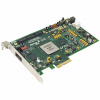
DK-DEV-1AGX60N
Manufacturer Part Number
DK-DEV-1AGX60N
Description
KIT DEV ARRIA GX 1AGX60N
Manufacturer
Altera
Series
Arria GXr
Type
FPGAr
Datasheet
1.EP1AGX20CF484C6N.pdf
(234 pages)
Specifications of DK-DEV-1AGX60N
Contents
Dev. Board, Quartus® II Web Edition, Reference Designs, Labs, and Complete Documentation
For Use With/related Products
1AGX60N
Lead Free Status / RoHS Status
Lead free / RoHS Compliant
Other names
544-2372
Available stocks
Company
Part Number
Manufacturer
Quantity
Price


Chapter 4: DC and Switching Characteristics
I/O Timing Model
Table 4–45. Timing Measurement Methodology for Input Pins
Clock Network Skew Adders
Table 4–46. Clock Network Specifications
Default Capacitive Loading of Different I/O Standards
© December 2009 Altera Corporation
Differential SSTL-18 Class II
1.5-V differential HSTL Class I
1.5-V differential HSTL Class II
1.8-V differential HSTL Class I
1.8-V differential HSTL Class II
LVDS
LVPECL
Notes to
(1) Input buffer sees no load at buffer input.
(2) Input measuring point at buffer input is 0.5 V
(3) Output measuring point is 0.5 V
(4) Input edge rate is 1 V/ns.
(5) Less than 50-mV ripple on V
(6) V
Clock skew adder
EP1AGX20/35
Clock skew adder
EP1AGX50/60
Clock skew adder
EP1AGX90
Note to
(1) This is in addition to intra-clock network skew, which is modeled in the Quartus II software.
CCPD
Table
Table
= 2.97 V, less than 50-mV ripple on V
Name
(1)
I/O Standard
4–46:
4–45:
(1)
(1)
The Quartus II software models skew within dedicated clock networks such as global
and regional clocks. Therefore, the intra-clock network skew adder is not specified.
Table 4–46
registers in the Arria GX device.
See
Table 4–47. Default Loading of Different I/O Standards for Arria GX Devices (Part 1 of 2)
LVTTL
LVCMOS
2.5 V
Inter-clock network, same side
Inter-clock network, entire chip
Inter-clock network, same side
Inter-clock network, entire chip
Inter-clock network, same side
Inter-clock network, entire chip
Table 4–47
CCIO
CC
and V
at internal node.
specifies the intra clock skew between any two clock networks driving any
CCPD
I/O Standard
, V
for default capacitive loading of different I/O standards.
CCIO
Description
CCIO
CCINT
V
and V
.
1.660
1.375
1.375
1.660
1.660
2.325
3.135
CCIO
= 1.15 V with less than 30-mV ripple.
CCPD
(V)
, V
Measurement Conditions
CCINT
= 1.15 V.
V
0.830
0.688
0.688
0.830
0.830
REF
(Note
—
—
(V)
Min
Capacitive Load
—
—
—
—
—
—
1), (2), (3),
Edge Rate (ns)
0
0
0
Typ
—
—
—
—
—
—
1.660
1.375
1.375
1.660
1.660
0.100
0.100
(4)
(Part 2 of 2)
± 100
± 100
± 110
± 50
Max
± 50
± 55
Arria GX Device Handbook, Volume 1
Measurement Point
Units
Units
VMEAS (V)
ps
ps
ps
ps
ps
ps
pF
pF
pF
0.6875
0.6875
1.1625
1.5675
0.83
0.83
0.83
4–31
Related parts for DK-DEV-1AGX60N
Image
Part Number
Description
Manufacturer
Datasheet
Request
R

Part Number:
Description:
KIT DEV ARRIA II GX FPGA 2AGX125
Manufacturer:
Altera
Datasheet:

Part Number:
Description:
KIT DEV CYCLONE III LS EP3CLS200
Manufacturer:
Altera
Datasheet:

Part Number:
Description:
KIT DEV STRATIX IV FPGA 4SE530
Manufacturer:
Altera
Datasheet:

Part Number:
Description:
KIT DEV FPGA 2AGX260 W/6.375G TX
Manufacturer:
Altera
Datasheet:

Part Number:
Description:
KIT DEV MAX V 5M570Z
Manufacturer:
Altera
Datasheet:

Part Number:
Description:
KIT DEV STRATIX V FPGA 5SGXEA7
Manufacturer:
Altera
Datasheet:

Part Number:
Description:
KIT DEVELOPMENT STRATIX III
Manufacturer:
Altera
Datasheet:

Part Number:
Description:
KIT DEVELOPMENT STRATIX IV
Manufacturer:
Altera
Datasheet:
Part Number:
Description:
KIT STARTER CYCLONE IV GX
Manufacturer:
Altera
Datasheet:
Part Number:
Description:
KIT DEVELOPMENT STRATIX IV
Manufacturer:
Altera
Datasheet:

Part Number:
Description:
CPLD, EP610 Family, ECMOS Process, 300 Gates, 16 Macro Cells, 16 Reg., 16 User I/Os, 5V Supply, 35 Speed Grade, 24DIP
Manufacturer:
Altera Corporation
Datasheet:
Part Number:
Description:
CPLD, EP610 Family, ECMOS Process, 300 Gates, 16 Macro Cells, 16 Reg., 16 User I/Os, 5V Supply, 15 Speed Grade, 24DIP
Manufacturer:
Altera Corporation
Datasheet: