DS3141+ Maxim Integrated Products, DS3141+ Datasheet - Page 9
DS3141+
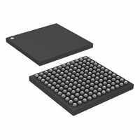
Manufacturer Part Number
DS3141+
Description
IC FRAMER DS3/E3 SNGL 144CSBGA
Manufacturer
Maxim Integrated Products
Datasheet
1.DS3141.pdf
(88 pages)
Specifications of DS3141+
Controller Type
DS3/E3 Framer
Interface
LIU
Voltage - Supply
3.135 V ~ 3.465 V
Current - Supply
80mA
Operating Temperature
-40°C ~ 85°C
Mounting Type
Surface Mount
Package / Case
144-CSBGA
Lead Free Status / RoHS Status
Lead free / RoHS Compliant


5. PIN DESCRIPTION
5.1 Transmit Formatter LIU Interface Pins
5.2 Receive Framer LIU Interface Pins
RPOS/
RNEG/
NAME
TPOS/
RNRZ
NAME
RLCV
RCLK
TNEG
TNRZ
TCLK
TYPE
I/O
I
I
I
O
O
O
Receive Positive Data Input/Receive NRZ Data Input. If BIN = 0 in the
dual-rail (POS/NEG) mode. In this mode, the framer clocks in the serial data stream in AMI format. RPOS =
1 from an external LIU indicates a positive pulse was received on the line; RNEG = 1 from the LIU indicates
a negative pulse was received on the line. If BIN = 1, the framer is in binary (NRZ) LIU interface mode. In
this mode the framer clocks in the serial data stream in binary format on the RNRZ pin. RNRZ = 1 indicates
a 1 in the data stream; RNRZ = 0 indicates a 0 in the data stream. If RCLKI = 0 in the
clocked into the framer on the rising edge of RCLK. If RCLKI = 1, data is clocked in on the falling edge of
RCLK. MC5:RPOSI = 1 inverts the polarity of RPOS/RNRZ.
Receive Negative Data Input/Receive Line-Code Violation Input. If BIN = 0 in the
interface is in dual-rail (POS/NEG) mode. In this mode, the framer clocks in the serial data stream in AMI
format. RPOS = 1 from an external LIU indicates a positive pulse was received on the line, while RNEG = 1
from the LIU indicates a negative pulse was received on the line. If BIN = 1, the framer is in binary (NRZ) LIU
interface mode. In this mode the framer clocks in the serial data stream in binary format on the RNRZ pin
and line code violations on the RLCV pin. If RCLKI = 0 in the
the rising edge of RCLK. If RCLKI = 1, data is clocked in on the falling edge of RCLK. MC5:RNEGI = 1
inverts the polarity of RNEG/RLCV. In binary LIU interface mode, when MC5:RNEGI = 0, the BPV counter
(registers
counter counts RCLK cycles when RLCV = 0.
Receive Clock Input. RCLK is used to clock data into the receive framer on RPOS/RNEG (dual-rail LIU
interface mode) or RNRZ (binary LIU interface mode). If RCLKI = 0 in the
the framer on the rising edge of RCLK. If RCLKI = 1, data is clocked in on the falling edge of RCLK. RCLK is
normally accurate to within ±20ppm when sourced from an LIU, but the framer can also accept a gapped
clock up to 52MHz on RCLK, such as those commonly sourced from ICs that map/demap DS3 and E3
to/from SONET/SDH.
Transmit Positive Data Output/Transmit NRZ Data Output. If BIN = 0 in the
is in dual-rail (POS/NEG) mode. In this mode, the transmit formatter outputs the serial data stream in
alternate mark inversion (AMI) format. TPOS = 1 signals an external LIU to drive a positive pulse on the
line, while TNEG = 1 tells the LIU to drive a negative pulse on the line. If BIN = 1, the LIU interface is in
binary (NRZ) mode. In this mode, the transmit formatter outputs the serial data stream in binary format on
the TNRZ pin. TNRZ = 1 indicates a 1 in the data stream, while TNRZ = 0 indicates a 0. If TCLKI = 0 in the
MC5
out on the falling edge of TCLK. MC5:TPOSH = 1 forces TPOS/TNRZ high. MC5:TPOSI = 1 inverts the
polarity of TPOS/TNRZ. Setting both TPOSH = 1 and TPOSI = 1 forces TPOS/TNRZ low.
Transmit Negative Data Output. If BIN = 0 in the
mode. In this mode, the transmit formatter outputs the serial data stream in AMI format. TPOS = 1 signals
an external LIU to drive a positive pulse on the line, while TNEG = 1 tells the LIU to drive a negative pulse
on the line. If BIN = 1, the LIU interface is in binary (NRZ) mode. In this mode the transmit formatter outputs
the serial data stream in binary format on the TNRZ pin, and TNEG is driven low. If TCLKI = 0 in the
register, data is clocked out of the formatter on the rising edge of TCLK. If TCLKI = 1, data is clocked out on
the falling edge of TCLK. MC5:TNEGH = 1 forces TNEG high. MC5:TNEGI = 1 inverts the polarity of TNEG.
Setting both TNEGH = 1 and TNEGI = 1 forces TNEG low.
Transmit Clock Output. TCLK is used to clock data out of the transmit formatter on TPOS/TNEG (dual-rail
LIU interface mode) or TNRZ (binary LIU interface mode). If TCLKI = 0 in the
out of the formatter on the rising edge of TCLK. If TCLKI = 1, data is clocked out on the falling edge of
TCLK. TCLK is normally a buffered (and optionally inverted) version of TICLK. When either line loopback or
payload loopback is active, TCLK is a buffered (and optionally inverted) version of RCLK. When a clock is
not present on TICLK and MC1:LOTCMC = 1, TCLK is a buffered (and optionally inverted) version of
RCLK.
register, data is clocked out of the formatter on the rising edge of TCLK. If TCLKI = 1, data is clocked
BPVCR1
and BPVCR2) counts RCLK cycles when RLCV = 1. When MC5:RNEGI = 1, the BPV
9 of 88
FUNCTION
FUNCTION
MC1
register, the LIU interface is in dual-rail (POS/NEG)
MC5
register, data is clocked into the framer on
MC1
MC5
register, the LIU interface is in
MC1
MC5
register, data is clocked into
MC1
register, the LIU interface
register, data is clocked
MC5
register, the LIU
register, data is
MC5
Related parts for DS3141+
Image
Part Number
Description
Manufacturer
Datasheet
Request
R

Part Number:
Description:
MAX7528KCWPMaxim Integrated Products [CMOS Dual 8-Bit Buffered Multiplying DACs]
Manufacturer:
Maxim Integrated Products
Datasheet:
Part Number:
Description:
Single +5V, fully integrated, 1.25Gbps laser diode driver.
Manufacturer:
Maxim Integrated Products
Datasheet:
Part Number:
Description:
Single +5V, fully integrated, 155Mbps laser diode driver.
Manufacturer:
Maxim Integrated Products
Datasheet:
Part Number:
Description:
VRD11/VRD10, K8 Rev F 2/3/4-Phase PWM Controllers with Integrated Dual MOSFET Drivers
Manufacturer:
Maxim Integrated Products
Datasheet:
Part Number:
Description:
Highly Integrated Level 2 SMBus Battery Chargers
Manufacturer:
Maxim Integrated Products
Datasheet:
Part Number:
Description:
Current Monitor and Accumulator with Integrated Sense Resistor; ; Temperature Range: -40°C to +85°C
Manufacturer:
Maxim Integrated Products
Part Number:
Description:
TSSOP 14/A�/RS-485 Transceivers with Integrated 100O/120O Termination Resis
Manufacturer:
Maxim Integrated Products
Part Number:
Description:
TSSOP 14/A�/RS-485 Transceivers with Integrated 100O/120O Termination Resis
Manufacturer:
Maxim Integrated Products
Part Number:
Description:
QFN 16/A�/AC-DC and DC-DC Peak-Current-Mode Converters with Integrated Step
Manufacturer:
Maxim Integrated Products
Part Number:
Description:
TDFN/A/65V, 1A, 600KHZ, SYNCHRONOUS STEP-DOWN REGULATOR WITH INTEGRATED SWI
Manufacturer:
Maxim Integrated Products
Part Number:
Description:
Integrated Temperature Controller f
Manufacturer:
Maxim Integrated Products
Part Number:
Description:
SOT23-6/I�/45MHz to 650MHz, Integrated IF VCOs with Differential Output
Manufacturer:
Maxim Integrated Products
Part Number:
Description:
SOT23-6/I�/45MHz to 650MHz, Integrated IF VCOs with Differential Output
Manufacturer:
Maxim Integrated Products
Part Number:
Description:
EVALUATION KIT/2.4GHZ TO 2.5GHZ 802.11G/B RF TRANSCEIVER WITH INTEGRATED PA
Manufacturer:
Maxim Integrated Products
Part Number:
Description:
QFN/E/DUAL PCIE/SATA HIGH SPEED SWITCH WITH INTEGRATED BIAS RESISTOR
Manufacturer:
Maxim Integrated Products
Datasheet: