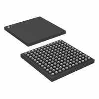
DS3141+ Maxim Integrated Products, DS3141+ Datasheet - Page 25

DS3141+
Manufacturer Part Number
DS3141+
Description
IC FRAMER DS3/E3 SNGL 144CSBGA
Manufacturer
Maxim Integrated Products
Datasheet
1.DS3141.pdf
(88 pages)
Specifications of DS3141+
Controller Type
DS3/E3 Framer
Interface
LIU
Voltage - Supply
3.135 V ~ 3.465 V
Current - Supply
80mA
Operating Temperature
-40°C ~ 85°C
Mounting Type
Surface Mount
Package / Case
144-CSBGA
Lead Free Status / RoHS Status
Lead free / RoHS Compliant
Register Name:
Register Description:
Register Address:
Bit #
Name
Default
Bit 0: TDEN Invert Enable (TDENI)
Bit 1: TDAT Invert Enable (TDATI)
Bit 2: TICLK Invert Enable (TICLKI)
Bit 3: TSOF Invert Enable (TSOFI)
Bit 4: TOH Invert Enable (TOHI)
Bit 5: TOHEN Invert Enable (TOHENI)
Bit 6: Transmit Start-of-Frame I/O Control (TSOFC). When this bit is logic 1, the TSOF pin is an output and
pulses for the last TICLK cycle of each frame. When this bit is 0, the TSOF pin is an input, and the device uses it to
determine the frame boundaries. See
Bit 7: Transmit Data-Enable Mode Select (TDENMS). When this bit is logic 0, the TDEN/TGCLK output has the
TDEN (data enable) function. TDEN asserts during payload bit times and de-asserts during overhead bit times.
When this bit is logic 1, TDEN/TGCLK has the TGCLK (gapped clock) function. TGCLK pulses during payload bit
times and is suppressed during overhead bit times. The TCCLK control bit in the
over this control bit. See
0 = do not invert the TDEN/TGCLK signal (normal mode)
1 = invert the TDEN/TGCLK signal (inverted mode)
0 = do not invert the TDAT signal (normal mode)
1 = invert the TDAT signal (inverted mode)
0 = do not invert the TICLK signal (normal mode)
1 = invert the TICLK signal (inverted mode)
0 = do not invert the TSOF signal (normal mode)
1 = invert the TSOF signal (inverted mode)
0 = do not invert the TOH signal (normal mode)
1 = invert the TOH signal (inverted mode)
0 = do not invert the TOHEN signal (normal mode)
1 = invert the TOHEN signal (inverted mode)
0 = TSOF is an input (reset default as input)
1 = TSOF is an output
0 = TDEN (data enable) mode
1 = TGCLK (gapped clock) mode
TDENMS
7
0
Figure 5-1
TSOFC
6
0
MC3
Master Configuration Register 3
03h
for functional timing information.
Figure 5-1
TOHENI
5
0
for functional timing information.
25 of 88
TOHI
4
0
TSOFI
3
0
TICLKI
2
0
MC2
register has precedence
TDATI
1
0
TDENI
0
0


