DS3141+ Maxim Integrated Products, DS3141+ Datasheet - Page 12
DS3141+
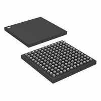
Manufacturer Part Number
DS3141+
Description
IC FRAMER DS3/E3 SNGL 144CSBGA
Manufacturer
Maxim Integrated Products
Datasheet
1.DS3141.pdf
(88 pages)
Specifications of DS3141+
Controller Type
DS3/E3 Framer
Interface
LIU
Voltage - Supply
3.135 V ~ 3.465 V
Current - Supply
80mA
Operating Temperature
-40°C ~ 85°C
Mounting Type
Surface Mount
Package / Case
144-CSBGA
Lead Free Status / RoHS Status
Lead free / RoHS Compliant


5.4 Receive Framer System Interface Pins
ROCLK
RGCLK
RDEN/
NAME
ROOF
RDAT
RSOF
RLOS
RECU
TYPE
O
O
O
O
O
O
I
Receive Output Clock. ROCLK is used to clock data out of the receive framer on RDAT. ROCLK is
normally a buffered (and optionally inverted) version of RCLK. When diagnostic loopback is active, ROCLK
is a buffered (and optionally inverted) version of TICLK. If MC4:ROCLKI = 0, data is clocked out of the
framer on the rising edge of ROCLK. If ROCLKI = 1, data is clocked out on the falling edge of ROCLK.
Receive Data Output. The incoming DS3/E3 data stream is serially clocked out of the receive framer on the
RDAT pin. RDAT is normally updated on the rising edge of ROCLK. To output data on the falling edge of
ROCLK, set MC4:ROCLKI = 1. To internally invert RDAT, set MC4:RDATI = 1. To force RDAT high, set
MC4:RDATH = 1. To force RDAT low, set MC4:RDATI = MC4:RDATH = 1.
Receive Data Enable/Receive Gapped Clock. The receive framer can be configured to either output a data
enable (RDEN) or a gapped clock (RGCLK). In data enable mode, RDEN goes active when payload data is
available on the RDAT output pin and inactive when overhead data is present on the RDAT pin. In gapped
clock mode, RGCLK acts as a payload data clock for the RDAT output, toggling for each payload bit
position and not toggling for each framing overhead bit position. In DS3 mode, overhead data is defined as
the M bits, F bits, C bits, X bits, and P bits. In E3 mode, overhead data is defined as the FAS word, RAI bit,
and Sn bit (bits 1 to 12). To configure the receive framer for data enable mode, set MC4:RDENMS = 0. To
configure for gapped clock operation, set MC4:RDENMS = 1. RDEN is normally active high; to make RDEN
active low, set MC4:RDENI = 1. RGCLK normally is the same polarity as RCLK; to invert RGCLK, set
MC4:RDENI = 1.
Receive Start of Frame. RSOF indicates the DS3 or E3 frame boundary on the incoming receive data
stream. RSOF pulses high for one TICLK cycle during the last bit of each DS3 or E3 frameRSOF is
normally active high. Set MC4:RSOFI = 1 to make RSOF active low.
Receive Loss of Signal. RLOS goes high when the receive framer is in a loss-of-signal (LOS) state. It
remains high as long as the LOS state persists and returns low when the framer exits the LOS state. See
Table 7-E
through the LOS status bit in the
Receive Out of Frame. ROOF goes high when the receive framer is in an out-of-frame (OOF) state. It
remains high as long as the OOF state persists and returns low when the framer synchronizes. See
7-E
the OOF status bit in the
Receive Error-Counter Update Strobe. Through the AECU control bit in the
configured to use this asynchronous input to initiate an update of the internal error counters in all the
framers on the device. A 0-to-1 transition on the RECU pin causes the device to load the error counter
registers with the latest internal error counts. This signal must be returned low before a subsequent update
of the error counters can occur. After toggling the RECU pin, the host processor must wait at least 100ns
before reading the error counter registers to allow the device time to load the registers. This signal is
logically ORed with the MECU control bit in MC1. If this signal is not used, it should be wired low.
and
Table 7-F
and
Table 7-F
for details on the set and clear criteria for this pin. OOF status is also available through
for details on the set and clear criteria for this pin. LOS status is also available
T3E3SR
T3E3SR
register.
12 of 88
register.
FUNCTION
MC1
register, the device can be
Table
Related parts for DS3141+
Image
Part Number
Description
Manufacturer
Datasheet
Request
R

Part Number:
Description:
MAX7528KCWPMaxim Integrated Products [CMOS Dual 8-Bit Buffered Multiplying DACs]
Manufacturer:
Maxim Integrated Products
Datasheet:
Part Number:
Description:
Single +5V, fully integrated, 1.25Gbps laser diode driver.
Manufacturer:
Maxim Integrated Products
Datasheet:
Part Number:
Description:
Single +5V, fully integrated, 155Mbps laser diode driver.
Manufacturer:
Maxim Integrated Products
Datasheet:
Part Number:
Description:
VRD11/VRD10, K8 Rev F 2/3/4-Phase PWM Controllers with Integrated Dual MOSFET Drivers
Manufacturer:
Maxim Integrated Products
Datasheet:
Part Number:
Description:
Highly Integrated Level 2 SMBus Battery Chargers
Manufacturer:
Maxim Integrated Products
Datasheet:
Part Number:
Description:
Current Monitor and Accumulator with Integrated Sense Resistor; ; Temperature Range: -40°C to +85°C
Manufacturer:
Maxim Integrated Products
Part Number:
Description:
TSSOP 14/A�/RS-485 Transceivers with Integrated 100O/120O Termination Resis
Manufacturer:
Maxim Integrated Products
Part Number:
Description:
TSSOP 14/A�/RS-485 Transceivers with Integrated 100O/120O Termination Resis
Manufacturer:
Maxim Integrated Products
Part Number:
Description:
QFN 16/A�/AC-DC and DC-DC Peak-Current-Mode Converters with Integrated Step
Manufacturer:
Maxim Integrated Products
Part Number:
Description:
TDFN/A/65V, 1A, 600KHZ, SYNCHRONOUS STEP-DOWN REGULATOR WITH INTEGRATED SWI
Manufacturer:
Maxim Integrated Products
Part Number:
Description:
Integrated Temperature Controller f
Manufacturer:
Maxim Integrated Products
Part Number:
Description:
SOT23-6/I�/45MHz to 650MHz, Integrated IF VCOs with Differential Output
Manufacturer:
Maxim Integrated Products
Part Number:
Description:
SOT23-6/I�/45MHz to 650MHz, Integrated IF VCOs with Differential Output
Manufacturer:
Maxim Integrated Products
Part Number:
Description:
EVALUATION KIT/2.4GHZ TO 2.5GHZ 802.11G/B RF TRANSCEIVER WITH INTEGRATED PA
Manufacturer:
Maxim Integrated Products
Part Number:
Description:
QFN/E/DUAL PCIE/SATA HIGH SPEED SWITCH WITH INTEGRATED BIAS RESISTOR
Manufacturer:
Maxim Integrated Products
Datasheet: