DS3141+ Maxim Integrated Products, DS3141+ Datasheet - Page 14
DS3141+
Manufacturer Part Number
DS3141+
Description
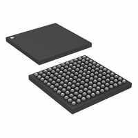
IC FRAMER DS3/E3 SNGL 144CSBGA
Manufacturer
Maxim Integrated Products
Datasheet
1.DS3141.pdf
(88 pages)
Specifications of DS3141+
Controller Type
DS3/E3 Framer
Interface
LIU
Voltage - Supply
3.135 V ~ 3.465 V
Current - Supply
80mA
Operating Temperature
-40°C ~ 85°C
Mounting Type
Surface Mount
Package / Case
144-CSBGA
Lead Free Status / RoHS Status
Lead free / RoHS Compliant


5.5 CPU Bus Interface Pins
5.6 JTAG Interface Pins
5.7 Supply, Test, and Reset Pins
NAME
WR (R/W)
RD (DS)
TEST
RST
JTCLK
NAME
NAME
JTRST
HIZ
V
V
D[7:0]
A[9:0]
SCLK
JTDO
JTMS
MOT
JTDI
ALE
DD
INT
SS
CS
I/O
I
I
I
I/O
I/O
I/O
O
O
I
I
I
I
I
I
I
I
I
I
I
Factory Test Enable (Active Low, Internal 10kW Pullup). This pin should be left open-circuited.
High-Z Control (Active Low, Internal 10kW Pullup). When this pin is low and JTRST is low, all outputs go to the
high-impedance mode. This pin can be left open-circuited by the user.
Digital Ground Reference. All V
Digital Positive Supply. 3.3V (±5%). All V
Global Hardware Reset (Active Low). When this pin is driven low, all the framers in the device are reset and all
the internal registers are forced to their default values. The device is held in the reset state as long as this pin
is low. The clocks (TICLK and RCLK) must be stable and in spec before this pin is driven high. The device
registers can be configured for operation after the reset is deactivated.
CPU Bus Data. The host processor accesses the devices’ internal registers through this bus. These pins
are outputs during reads and inputs otherwise. D7 is the MSB; D0 is the LSB.
CPU Bus Address. The host processor specifies the address of the internal register to be accessed by this
bus. Pins A[9:8] specify the framer to be accessed. In multiplexed bus applications, the A[7:0] pins should
be connected to the D[7:0] pins, and A[9:0] must have a valid register address when the ALE pin goes low.
A9 is the MSB; A0 is the LSB.
CPU Bus Address Latch Enable. This pin controls the address latch for the A[9:0] inputs. When ALE is high,
the latch is transparent. On the falling edge of ALE, the latch samples and holds the A[9:0] inputs. In
nonmultiplexed bus applications, ALE should be wired high. In multiplexed bus applications, A[7:0] should
be connected to D[7:0], and the falling edge of ALE latches the address.
CPU Bus Chip Select, Active Low. The host processor selects the device for read or write access by driving
this pin low.
CPU Bus Read Enable (CPU Bus Data Strobe), Active Low. In Intel mode (MOT = 0), RD controls read
accesses to the device. In Motorola mode (MOT = 1), DS controls both read and write accesses to the
device, while the R/W pin specifies the type of access.
CPU Bus Interrupt, Open Drain, Active Low. This pin is driven low by the device if one or more unmasked
interrupt sources within the device are active. INT remains low until the interrupt is serviced or masked.
System Clock. An ungapped clock with frequency between 33MHz and 52MHz must be provided to this pin
to run certain logic in the CPU bus port. The use of this clock allows the transmit and receive clocks (TICLK
and RCLK) to be gapped, if desired, without affecting the CPU bus timing. This pin can be connected to
TICLK or RCLK if the signal on one of those pins is an ungapped clock.
JTAG IEEE 1149.1 Test Serial-Data Input (Internal 10kW Pullup). Test instructions and data are clocked in
on this pin on the rising edge of JTCLK. If not used, JTDI should be left unconnected or driven high.
JTAG IEEE 1149.1 Test Serial-Data Output. Test instructions are clocked out of this pin on the falling edge
of JTCLK. If not used, JTDO should be left open-circuited. This pin is in tri-state mode after JTRST is
activated.
JTAG IEEE 1149.1 Test Reset (Active Low, Internal 10kW Pullup). This pin is used to asynchronously reset
the test access port controller. At power-up, JTRST must be driven low and then high. This action sets the
device into the boundary scan bypass mode, allowing normal device operation. If boundary scan is not
used, this pin should be held low.
JTAG IEEE 1149.1 Test Mode Select (Internal 10kW Pullup). This pin is sampled on the rising edge of
JTCLK and is used to place the test port into the various defined IEEE 1149.1 states. If not used, JTMS
should be left unconnected or driven high.
Motorola Bus Mode Select. This pin controls whether the CPU bus operates in Intel mode or in Motorola
mode.
0 = CPU bus is in Intel mode
1 = CPU bus is in Motorola mode
JTAG IEEE 1149.1 Test Serial Clock. This pin is used to shift data into JTDI on the rising edge and out of
JTDO on the falling edge. If not used, this pin should be wired high.
CPU Bus Write Enable (CPU Bus Read/Write Select), Active Low. In Intel mode (MOT = 0), WR controls
write accesses to the device. In Motorola mode (MOT = 1), R/W specifies whether a read or a write access
is to occur.
SS
pins should be wired together.
DD
14 of 88
pins should be wired together.
FUNCTION
FUNCTION
FUNCTION
Related parts for DS3141+
Image
Part Number
Description
Manufacturer
Datasheet
Request
R

Part Number:
Description:
MAX7528KCWPMaxim Integrated Products [CMOS Dual 8-Bit Buffered Multiplying DACs]
Manufacturer:
Maxim Integrated Products
Datasheet:
Part Number:
Description:
Single +5V, fully integrated, 1.25Gbps laser diode driver.
Manufacturer:
Maxim Integrated Products
Datasheet:
Part Number:
Description:
Single +5V, fully integrated, 155Mbps laser diode driver.
Manufacturer:
Maxim Integrated Products
Datasheet:
Part Number:
Description:
VRD11/VRD10, K8 Rev F 2/3/4-Phase PWM Controllers with Integrated Dual MOSFET Drivers
Manufacturer:
Maxim Integrated Products
Datasheet:
Part Number:
Description:
Highly Integrated Level 2 SMBus Battery Chargers
Manufacturer:
Maxim Integrated Products
Datasheet:
Part Number:
Description:
Current Monitor and Accumulator with Integrated Sense Resistor; ; Temperature Range: -40°C to +85°C
Manufacturer:
Maxim Integrated Products
Part Number:
Description:
TSSOP 14/A�/RS-485 Transceivers with Integrated 100O/120O Termination Resis
Manufacturer:
Maxim Integrated Products
Part Number:
Description:
TSSOP 14/A�/RS-485 Transceivers with Integrated 100O/120O Termination Resis
Manufacturer:
Maxim Integrated Products
Part Number:
Description:
QFN 16/A�/AC-DC and DC-DC Peak-Current-Mode Converters with Integrated Step
Manufacturer:
Maxim Integrated Products
Part Number:
Description:
TDFN/A/65V, 1A, 600KHZ, SYNCHRONOUS STEP-DOWN REGULATOR WITH INTEGRATED SWI
Manufacturer:
Maxim Integrated Products
Part Number:
Description:
Integrated Temperature Controller f
Manufacturer:
Maxim Integrated Products
Part Number:
Description:
SOT23-6/I�/45MHz to 650MHz, Integrated IF VCOs with Differential Output
Manufacturer:
Maxim Integrated Products
Part Number:
Description:
SOT23-6/I�/45MHz to 650MHz, Integrated IF VCOs with Differential Output
Manufacturer:
Maxim Integrated Products
Part Number:
Description:
EVALUATION KIT/2.4GHZ TO 2.5GHZ 802.11G/B RF TRANSCEIVER WITH INTEGRATED PA
Manufacturer:
Maxim Integrated Products
Part Number:
Description:
QFN/E/DUAL PCIE/SATA HIGH SPEED SWITCH WITH INTEGRATED BIAS RESISTOR
Manufacturer:
Maxim Integrated Products
Datasheet: