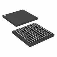
DS3141+ Maxim Integrated Products, DS3141+ Datasheet - Page 67

DS3141+
Manufacturer Part Number
DS3141+
Description
IC FRAMER DS3/E3 SNGL 144CSBGA
Manufacturer
Maxim Integrated Products
Datasheet
1.DS3141.pdf
(88 pages)
Specifications of DS3141+
Controller Type
DS3/E3 Framer
Interface
LIU
Voltage - Supply
3.135 V ~ 3.465 V
Current - Supply
80mA
Operating Temperature
-40°C ~ 85°C
Mounting Type
Surface Mount
Package / Case
144-CSBGA
Lead Free Status / RoHS Status
Lead free / RoHS Compliant
8. OPERATION DETAILS
8.1 Reset
The DS314x devices must be reset by activating the JTRST and RST pins after the power supply has settled and
the input clocks have stabilized to their normal operating conditions. The JTRST pin can be permanently wired low
if desired. After reset, all read/write control register bits are reset to 0 except for RDATH and TUA1, which are set
to 1. The reset states of the device pins are as follows:
8.2 DS3 and E3 Mode Configuration
In all modes, the TUA1 bit in the
set to 1 at reset to generate an unframed all-ones (E3 AIS) signal on both the transmit LIU interface (TPOS/TNEG)
and the receive system interface (RDAT).
E3 Mode
Default framer operation after reset is E3 mode. To begin operation in E3 mode after reset, clear the TUA1 bit in
the
pin.
DS3 M23 Mode
To change framer operation after reset to DS3 M23 mode, set the DS3M bit to 1 in the
TUA1 bit in the
the TICLK pin.
DS3 C-Bit Parity Mode
To change framer operation after reset to DS3 C-Bit Parity mode, set the DS3M and CBEN bits to 1 in the
T3E3CR1
44.736MHz clock must be applied to the TICLK pin.
8.3 LIU and System Interface Configuration
LIU Interface
After reset the default LIU interface format is dual-rail (POS/NEG) with B3ZS/HDB3 encoding and decoding
enabled. To change framer operation after reset to binary (NRZ) format with B3ZS/HDB3 encoding and decoding
disabled (disabled in the framer but should be enabled in the LIU), set the BIN bit to 1 in the
System Interface
After reset the TDEN/TGCLK and RDEN/RGCLK pins default to data enable behavior (TDEN, RDEN) and the
TSOF pin defaults to being an input. If gapped clock behavior is desired, set the TDENMS bit tin the
and/or the RDENMS bit in the
MC3
·
·
·
·
·
·
·
·
·
·
·
MC1
E3 mode is enabled.
The LIU interface is in dual-rail (POS/NEG) mode with HDB3 encoding and decoding enabled.
TPOS and TNEG transmit an unframed all-ones signal (E3 AIS) on the transmit LIU interface.
RDAT is forced to a logic 1 level to present an unframed all-ones signal (E3 AIS) on the receive system
interface.
TCLK is a noninverted, delayed version of TICLK.
ROCLK is a noninverted, delayed version or RCLK.
TSOF is an active-high input pin.
RSOF, RLOS, and ROOF are active high.
TDEN/TGCLK is in the TDEN (data enable) mode and is active high.
RDEN/RGCLK is in the RDEN (data enable) mode and is active high.
JTDO is tri-stated.
register.
register and clear the RDATH bit in the
register, clear the TUA1 bit in the
MC1
register, and clear the RDATH bit in the
MC4
MC1
register. To configure TSOF as an output pin, set the TSOFC bit to 1 in the
register and RDATH bit in the
MC1
MC4
67 of 88
register, and clear the RDATH bit in the
register. A 34.368MHz clock must be applied to the TICLK
MC4
register. A 44.736MHz clock must be applied to
MC4
register must be cleared. These bits are
T3E3CR1
MC1
register.
register, clear the
MC4
MC3
register. A
register


