DS3141+ Maxim Integrated Products, DS3141+ Datasheet - Page 27
DS3141+
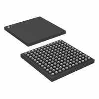
Manufacturer Part Number
DS3141+
Description
IC FRAMER DS3/E3 SNGL 144CSBGA
Manufacturer
Maxim Integrated Products
Datasheet
1.DS3141.pdf
(88 pages)
Specifications of DS3141+
Controller Type
DS3/E3 Framer
Interface
LIU
Voltage - Supply
3.135 V ~ 3.465 V
Current - Supply
80mA
Operating Temperature
-40°C ~ 85°C
Mounting Type
Surface Mount
Package / Case
144-CSBGA
Lead Free Status / RoHS Status
Lead free / RoHS Compliant


Register Name:
Register Description:
Register Address:
Bit #
Name
Default
Bit 0: TCLK Invert Enable (TCLKI)
Bit 1: TPOS/TNRZ Invert Enable (TPOSI)
Bit 2: TNEG Invert Enable (TNEGI)
Bit 3: TPOS/TNRZ Force-High Enable (TPOSH). The TPOS/TNRZ pin can be forced low by setting both the
TPOSH and TPOSI control bits.
Bit 4: TNEG Force-High Enable (TNEGH). The TNEG pin can be forced low by setting both the TNEGH and
TNEGI control bits.
Bit 5: RCLK Invert Enable (RCLKI)
Bit 6: RPOS/RNRZ Invert Enable (RPOSI)
Bit 7: RNEG/RLCV Invert Enable (RNEGI)
Register Name:
Register Description:
Register Address:
Bit #
Name
Default
This register is a global resource and is mapped into address 06h in every framer in the device. In both interrupt-based and polling-based
device servicing strategies, the host processor should read this register first to determine which framers require servicing.
Bit 0: Interrupt 1 (INT1). This bit is set when framer 1 is driving the INT pin.
Bit 1: Interrupt 2 (INT2). This bit is set when framer 2 is driving the INT pin.
Bit 2: Interrupt 3 (INT3). This bit is set when framer 3 is driving the INT pin.
Bit 3: Interrupt 4 (INT4). This bit is set when framer 4 is driving the INT pin.
0 = do not invert the TCLK signal (normal mode)
1 = invert the TCLK signal (inverted mode)
0 = do not invert the TPOS/TNRZ signal (normal mode)
1 = invert the TPOS/TNRZ signal (inverted mode)
0 = do not invert the TNEG signal (normal mode)
1 = invert the TNEG signal (inverted mode)
0 = allow normal transmit data to appear at the TPOS/TNRZ pin (normal mode)
1 = force the TPOS/TNRZ signal high (force high mode, can be inverted)
0 = allow normal transmit data to appear at the TNEG pin (normal mode)
1 = force the TNEG signal high (force high mode, can be inverted)
0 = do not invert the RCLK signal (normal mode)
1 = invert the RCLK signal (inverted mode)
0 = do not invert the RPOS/RNRZ signal (normal mode)
1 = invert the RPOS/RNRZ signal (inverted mode)
0 = do not invert the RNEG/RLCV signal (normal mode)
1 = invert the RNEG/RLCV signal (inverted mode)
RNEGI
N/A
7
0
—
7
RPOSI
6
0
N/A
—
6
ISR1
Interrupt Status Register 1
06h
MC5
Master Configuration Register 5
05h
RCLKI
5
0
N/A
—
5
TNEGH
27 of 88
N/A
4
0
—
4
TPOSH
INT4
—
3
0
3
TNEGI
INT3
—
2
0
2
TPOSI
INT2
—
1
0
1
TCLKI
INT1
—
0
0
0
Related parts for DS3141+
Image
Part Number
Description
Manufacturer
Datasheet
Request
R

Part Number:
Description:
MAX7528KCWPMaxim Integrated Products [CMOS Dual 8-Bit Buffered Multiplying DACs]
Manufacturer:
Maxim Integrated Products
Datasheet:
Part Number:
Description:
Single +5V, fully integrated, 1.25Gbps laser diode driver.
Manufacturer:
Maxim Integrated Products
Datasheet:
Part Number:
Description:
Single +5V, fully integrated, 155Mbps laser diode driver.
Manufacturer:
Maxim Integrated Products
Datasheet:
Part Number:
Description:
VRD11/VRD10, K8 Rev F 2/3/4-Phase PWM Controllers with Integrated Dual MOSFET Drivers
Manufacturer:
Maxim Integrated Products
Datasheet:
Part Number:
Description:
Highly Integrated Level 2 SMBus Battery Chargers
Manufacturer:
Maxim Integrated Products
Datasheet:
Part Number:
Description:
Current Monitor and Accumulator with Integrated Sense Resistor; ; Temperature Range: -40°C to +85°C
Manufacturer:
Maxim Integrated Products
Part Number:
Description:
TSSOP 14/A�/RS-485 Transceivers with Integrated 100O/120O Termination Resis
Manufacturer:
Maxim Integrated Products
Part Number:
Description:
TSSOP 14/A�/RS-485 Transceivers with Integrated 100O/120O Termination Resis
Manufacturer:
Maxim Integrated Products
Part Number:
Description:
QFN 16/A�/AC-DC and DC-DC Peak-Current-Mode Converters with Integrated Step
Manufacturer:
Maxim Integrated Products
Part Number:
Description:
TDFN/A/65V, 1A, 600KHZ, SYNCHRONOUS STEP-DOWN REGULATOR WITH INTEGRATED SWI
Manufacturer:
Maxim Integrated Products
Part Number:
Description:
Integrated Temperature Controller f
Manufacturer:
Maxim Integrated Products
Part Number:
Description:
SOT23-6/I�/45MHz to 650MHz, Integrated IF VCOs with Differential Output
Manufacturer:
Maxim Integrated Products
Part Number:
Description:
SOT23-6/I�/45MHz to 650MHz, Integrated IF VCOs with Differential Output
Manufacturer:
Maxim Integrated Products
Part Number:
Description:
EVALUATION KIT/2.4GHZ TO 2.5GHZ 802.11G/B RF TRANSCEIVER WITH INTEGRATED PA
Manufacturer:
Maxim Integrated Products
Part Number:
Description:
QFN/E/DUAL PCIE/SATA HIGH SPEED SWITCH WITH INTEGRATED BIAS RESISTOR
Manufacturer:
Maxim Integrated Products
Datasheet: