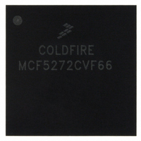
MCF5272CVF66 Freescale Semiconductor, MCF5272CVF66 Datasheet - Page 514

MCF5272CVF66
Manufacturer Part Number
MCF5272CVF66
Description
IC MPU 32BIT 66MHZ 196-MAPBGA
Manufacturer
Freescale Semiconductor
Series
MCF527xr
Specifications of MCF5272CVF66
Core Processor
Coldfire V2
Core Size
32-Bit
Speed
66MHz
Connectivity
EBI/EMI, Ethernet, I²C, SPI, UART/USART, USB
Peripherals
DMA, WDT
Number Of I /o
32
Program Memory Size
16KB (4K x 32)
Program Memory Type
ROM
Ram Size
1K x 32
Voltage - Supply (vcc/vdd)
3 V ~ 3.6 V
Oscillator Type
External
Operating Temperature
-40°C ~ 85°C
Package / Case
196-MAPBGA
Family Name
MCF5xxx
Device Core
ColdFire
Device Core Size
32b
Frequency (max)
66MHz
Instruction Set Architecture
RISC
Supply Voltage 1 (typ)
3.3V
Operating Temp Range
-40C to 85C
Operating Temperature Classification
Industrial
Mounting
Surface Mount
Pin Count
196
Package Type
MA-BGA
Lead Free Status / RoHS Status
Contains lead / RoHS non-compliant
Eeprom Size
-
Data Converters
-
Lead Free Status / Rohs Status
Not Compliant
Available stocks
Company
Part Number
Manufacturer
Quantity
Price
Company:
Part Number:
MCF5272CVF66
Manufacturer:
Freescale Semiconductor
Quantity:
10 000
Part Number:
MCF5272CVF66
Manufacturer:
FREESCALE
Quantity:
20 000
Company:
Part Number:
MCF5272CVF66 K75N
Manufacturer:
ST
Quantity:
18
Company:
Part Number:
MCF5272CVF66J
Manufacturer:
Freescale Semiconductor
Quantity:
10 000
- Current page: 514 of 544
- Download datasheet (7Mb)
Electrical Characteristics
23.12 IEEE 1149.1 (JTAG) AC Timing Specifications
Table 23-23
Figure 23-23
23-30
Name
J2a
J2b
J3a
J3b
J10
J11
J12
—
J1
J4
J5
J6
J7
J8
J9
TCK frequency of operation
TCK cycle time
TCK clock pulse high width measured at 1.5 V
TCK clock pulse low width measured at 1.5 V
TCK fall time (from V
TCK rise time (from V
TDI, TMS to TCK rising (setup)
TCK rising edge to TDI, TMS invalid (hold)
Boundary scan data valid to TCK rising edge (setup)
Boundary scan data invalid to TCK rising edge (hold)
TRST pulse-width (asynchronous to clock edges)
TCK falling edge to TDO valid (signal from driven or three-state)
TCK falling edge to TDO high impedance
TCK falling edge to boundary scan data valid (signal from driven or three-state)
TCK falling edge to boundary scan data high impedance
lists JTAG timings.
shows JTAG timings listed in
MCF5272 ColdFire
Scan Data
Scan Data
Boundary
Boundary
TDI, TMS
Table 23-23. IEEE 1149.1 (JTAG) AC Timing Specifications
Outputs
h
Inputs
TRST
l
TDO
= 2.4 V to V
TCK
= 0.5 V to V
J2a
Figure 23-23. IEEE 1149.1 (JTAG) Timing
J11
J9
l
h
J4
J6
= 0.5 V)
Characteristic
= 2.4 V)
®
Integrated Microprocessor User’s Manual, Rev. 3
J1
Table
23-23.
J8
J5
J7
J3a
J10
J12
J2b
V
V
h
l
J3b
Min
100
40
40
—
—
10
15
10
15
15
—
—
—
—
Freescale Semiconductor
0
0–66 MHz
Max
10
30
30
35
35
—
—
—
—
—
—
—
—
5
5
MHz
Unit
nS
nS
nS
nS
nS
nS
nS
nS
nS
nS
nS
nS
nS
nS
Related parts for MCF5272CVF66
Image
Part Number
Description
Manufacturer
Datasheet
Request
R
Part Number:
Description:
Mcf5272 Coldfire Integrated Microprocessor User
Manufacturer:
Freescale Semiconductor, Inc
Datasheet:

Part Number:
Description:
MCF5272 Interrupt Service Routine for the Physical Layer Interface Controller
Manufacturer:
Freescale Semiconductor / Motorola
Datasheet:
Part Number:
Description:
Manufacturer:
Freescale Semiconductor, Inc
Datasheet:
Part Number:
Description:
Manufacturer:
Freescale Semiconductor, Inc
Datasheet:
Part Number:
Description:
Manufacturer:
Freescale Semiconductor, Inc
Datasheet:
Part Number:
Description:
Manufacturer:
Freescale Semiconductor, Inc
Datasheet:
Part Number:
Description:
Manufacturer:
Freescale Semiconductor, Inc
Datasheet:
Part Number:
Description:
Manufacturer:
Freescale Semiconductor, Inc
Datasheet:
Part Number:
Description:
Manufacturer:
Freescale Semiconductor, Inc
Datasheet:
Part Number:
Description:
Manufacturer:
Freescale Semiconductor, Inc
Datasheet:
Part Number:
Description:
Manufacturer:
Freescale Semiconductor, Inc
Datasheet:
Part Number:
Description:
Manufacturer:
Freescale Semiconductor, Inc
Datasheet:
Part Number:
Description:
Manufacturer:
Freescale Semiconductor, Inc
Datasheet:
Part Number:
Description:
Manufacturer:
Freescale Semiconductor, Inc
Datasheet:
Part Number:
Description:
Manufacturer:
Freescale Semiconductor, Inc
Datasheet:


