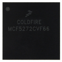
MCF5272CVF66 Freescale Semiconductor, MCF5272CVF66 Datasheet - Page 313

MCF5272CVF66
Manufacturer Part Number
MCF5272CVF66
Description
IC MPU 32BIT 66MHZ 196-MAPBGA
Manufacturer
Freescale Semiconductor
Series
MCF527xr
Specifications of MCF5272CVF66
Core Processor
Coldfire V2
Core Size
32-Bit
Speed
66MHz
Connectivity
EBI/EMI, Ethernet, I²C, SPI, UART/USART, USB
Peripherals
DMA, WDT
Number Of I /o
32
Program Memory Size
16KB (4K x 32)
Program Memory Type
ROM
Ram Size
1K x 32
Voltage - Supply (vcc/vdd)
3 V ~ 3.6 V
Oscillator Type
External
Operating Temperature
-40°C ~ 85°C
Package / Case
196-MAPBGA
Family Name
MCF5xxx
Device Core
ColdFire
Device Core Size
32b
Frequency (max)
66MHz
Instruction Set Architecture
RISC
Supply Voltage 1 (typ)
3.3V
Operating Temp Range
-40C to 85C
Operating Temperature Classification
Industrial
Mounting
Surface Mount
Pin Count
196
Package Type
MA-BGA
Lead Free Status / RoHS Status
Contains lead / RoHS non-compliant
Eeprom Size
-
Data Converters
-
Lead Free Status / Rohs Status
Not Compliant
Available stocks
Company
Part Number
Manufacturer
Quantity
Price
Company:
Part Number:
MCF5272CVF66
Manufacturer:
Freescale Semiconductor
Quantity:
10 000
Part Number:
MCF5272CVF66
Manufacturer:
FREESCALE
Quantity:
20 000
Company:
Part Number:
MCF5272CVF66 K75N
Manufacturer:
ST
Quantity:
18
Company:
Part Number:
MCF5272CVF66J
Manufacturer:
Freescale Semiconductor
Quantity:
10 000
- Current page: 313 of 544
- Download datasheet (7Mb)
13.5.4
All bits in these registers are read/write and are set on hardware or software reset.
The PnB1TR registers contain four frames of transmit data for channel B1. (P0B1TR is the B1 channel
transmit data for port 0, P1B1TR is B1 transmit for port 1, and so on.) The data are packed from LSB to
MSB.
These registers are aligned on long-word boundaries from MBAR + 0x328 for P0B1TR to
MBAR + 0x334 for P3B1TR. See
frame and bit alignment within the 32-bit word.
13.5.5
All bits in these registers are read/write and are set on hardware or software reset.
The PnB2TR registers contain four frames of transmit data for port n of channel B2. (P0B2TR is the B2
channel transmit data for port 0, P1B2TR is B2 transmit for port 1, and so on.) The data are packed from
LSB to MSB.
These registers are aligned on long-word boundaries from MBAR + 0x338 for P0B2TR to
MBAR + 0x344 for P3B2TR. Please refer to
for the frame and bit alignment within the 32-bit word.
Freescale Semiconductor
Reset
Reset
Reset
Reset
Field
Field
Field
Field
Addr
Addr
R/W
R/W
R/W
R/W
B1 Data Transmit Registers (P0B1TR–P3B1TR)
31
15
B2 Data Transmit Registers (P0B2TR–P3B2TR)
31
15
MCF5272 ColdFire
MBAR + 0x328 (P0B1TR); 0x32C (P1B1TR); 0x330 (P2B1TR); 0x334 (P3B1TR)
MBAR + 0x338 (P0B2TR); 0x33C (P1B2TR); 0x340 (P2B2TR); 0x344 (P3B2TR)
Figure 13-16. B1 Transmit Data Registers P0B1TR–P3B1TR
Figure 13-17. B2 Transmit Data Registers P0B2TR–P3B2TR
1111_1111
1111_1111
1111_1111
1111_1111
Frame 0
Frame 2
Frame0
Frame2
Section 13.2.3, “GCI/IDL B- and D-Channel Bit
®
Integrated Microprocessor User’s Manual, Rev. 3
Section 13.2.3, “GCI/IDL B- and D-Channel Bit
Read/Write
Read/Write
Read/Write
Read/Write
24
24
8
8
23
23
7
7
Physical Layer Interface Controller (PLIC)
1111_1111
1111_1111
1111_1111
1111_1111
Frame 1
Frame 3
Frame1
Frame3
Alignment,” for the
Alignment”
16
16
0
0
13-17
Related parts for MCF5272CVF66
Image
Part Number
Description
Manufacturer
Datasheet
Request
R
Part Number:
Description:
Mcf5272 Coldfire Integrated Microprocessor User
Manufacturer:
Freescale Semiconductor, Inc
Datasheet:

Part Number:
Description:
MCF5272 Interrupt Service Routine for the Physical Layer Interface Controller
Manufacturer:
Freescale Semiconductor / Motorola
Datasheet:
Part Number:
Description:
Manufacturer:
Freescale Semiconductor, Inc
Datasheet:
Part Number:
Description:
Manufacturer:
Freescale Semiconductor, Inc
Datasheet:
Part Number:
Description:
Manufacturer:
Freescale Semiconductor, Inc
Datasheet:
Part Number:
Description:
Manufacturer:
Freescale Semiconductor, Inc
Datasheet:
Part Number:
Description:
Manufacturer:
Freescale Semiconductor, Inc
Datasheet:
Part Number:
Description:
Manufacturer:
Freescale Semiconductor, Inc
Datasheet:
Part Number:
Description:
Manufacturer:
Freescale Semiconductor, Inc
Datasheet:
Part Number:
Description:
Manufacturer:
Freescale Semiconductor, Inc
Datasheet:
Part Number:
Description:
Manufacturer:
Freescale Semiconductor, Inc
Datasheet:
Part Number:
Description:
Manufacturer:
Freescale Semiconductor, Inc
Datasheet:
Part Number:
Description:
Manufacturer:
Freescale Semiconductor, Inc
Datasheet:
Part Number:
Description:
Manufacturer:
Freescale Semiconductor, Inc
Datasheet:
Part Number:
Description:
Manufacturer:
Freescale Semiconductor, Inc
Datasheet:


