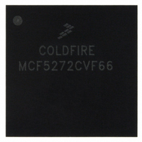
MCF5272CVF66 Freescale Semiconductor, MCF5272CVF66 Datasheet - Page 241

MCF5272CVF66
Manufacturer Part Number
MCF5272CVF66
Description
IC MPU 32BIT 66MHZ 196-MAPBGA
Manufacturer
Freescale Semiconductor
Series
MCF527xr
Specifications of MCF5272CVF66
Core Processor
Coldfire V2
Core Size
32-Bit
Speed
66MHz
Connectivity
EBI/EMI, Ethernet, I²C, SPI, UART/USART, USB
Peripherals
DMA, WDT
Number Of I /o
32
Program Memory Size
16KB (4K x 32)
Program Memory Type
ROM
Ram Size
1K x 32
Voltage - Supply (vcc/vdd)
3 V ~ 3.6 V
Oscillator Type
External
Operating Temperature
-40°C ~ 85°C
Package / Case
196-MAPBGA
Family Name
MCF5xxx
Device Core
ColdFire
Device Core Size
32b
Frequency (max)
66MHz
Instruction Set Architecture
RISC
Supply Voltage 1 (typ)
3.3V
Operating Temp Range
-40C to 85C
Operating Temperature Classification
Industrial
Mounting
Surface Mount
Pin Count
196
Package Type
MA-BGA
Lead Free Status / RoHS Status
Contains lead / RoHS non-compliant
Eeprom Size
-
Data Converters
-
Lead Free Status / Rohs Status
Not Compliant
Available stocks
Company
Part Number
Manufacturer
Quantity
Price
Company:
Part Number:
MCF5272CVF66
Manufacturer:
Freescale Semiconductor
Quantity:
10 000
Part Number:
MCF5272CVF66
Manufacturer:
FREESCALE
Quantity:
20 000
Company:
Part Number:
MCF5272CVF66 K75N
Manufacturer:
ST
Quantity:
18
Company:
Part Number:
MCF5272CVF66J
Manufacturer:
Freescale Semiconductor
Quantity:
10 000
- Current page: 241 of 544
- Download datasheet (7Mb)
11.5.13 Receive Control Register (RCR)
The RCR register,
Table 11-20
Freescale Semiconductor
31–4
Bits
Reset
Reset
3
2
1
0
Field
Field
Addr
R/W
R/W
31
15
describes the RCR fields.
MII_MODE
PROM
Name
LOOP
DRT
Figure
—
MCF5272 ColdFire
11-17, controls the operational mode of the receive block.
Reserved, should be cleared.
Promiscuous mode. All frames are accepted regardless of address matching.
MII mode enable. Selects the external interface mode. Setting this bit to one selects MII
mode, setting this bit equal to zero selects seven-wire mode (used only for serial 10 Mbps).
This bit controls the interface mode for both transmit and receive blocks.
Disable receive on transmit
0 Receive path operates independently of transmit (use for full duplex or to monitor transmit
activity in half-duplex mode).
1 Disable reception of frames while transmitting (normally used for half-duplex mode).
Internal loopback. If set, transmitted frames are looped back internal to the FEC and the
transmit output signals are not asserted. The system clock is substituted for the E_TxCLK
when LOOP is asserted. DRT must be set to zero when asserting LOOP.
Figure 11-17. Receive Control Register (RCR)
Table 11-20. RCR Field Descriptions
®
Integrated Microprocessor User’s Manual, Rev. 3
—
0000_0000_0000_0000
0000_0000_0000_0000
MBAR + 0x944
Read/Write
Read/Write
—
Description
4
PROM MII_MODE DRT LOOP
3
2
1
Ethernet Module
16
0
11-23
Related parts for MCF5272CVF66
Image
Part Number
Description
Manufacturer
Datasheet
Request
R
Part Number:
Description:
Mcf5272 Coldfire Integrated Microprocessor User
Manufacturer:
Freescale Semiconductor, Inc
Datasheet:

Part Number:
Description:
MCF5272 Interrupt Service Routine for the Physical Layer Interface Controller
Manufacturer:
Freescale Semiconductor / Motorola
Datasheet:
Part Number:
Description:
Manufacturer:
Freescale Semiconductor, Inc
Datasheet:
Part Number:
Description:
Manufacturer:
Freescale Semiconductor, Inc
Datasheet:
Part Number:
Description:
Manufacturer:
Freescale Semiconductor, Inc
Datasheet:
Part Number:
Description:
Manufacturer:
Freescale Semiconductor, Inc
Datasheet:
Part Number:
Description:
Manufacturer:
Freescale Semiconductor, Inc
Datasheet:
Part Number:
Description:
Manufacturer:
Freescale Semiconductor, Inc
Datasheet:
Part Number:
Description:
Manufacturer:
Freescale Semiconductor, Inc
Datasheet:
Part Number:
Description:
Manufacturer:
Freescale Semiconductor, Inc
Datasheet:
Part Number:
Description:
Manufacturer:
Freescale Semiconductor, Inc
Datasheet:
Part Number:
Description:
Manufacturer:
Freescale Semiconductor, Inc
Datasheet:
Part Number:
Description:
Manufacturer:
Freescale Semiconductor, Inc
Datasheet:
Part Number:
Description:
Manufacturer:
Freescale Semiconductor, Inc
Datasheet:
Part Number:
Description:
Manufacturer:
Freescale Semiconductor, Inc
Datasheet:


