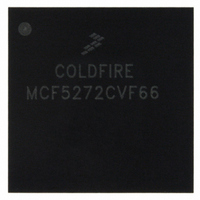
MCF5272CVF66 Freescale Semiconductor, MCF5272CVF66 Datasheet - Page 191

MCF5272CVF66
Manufacturer Part Number
MCF5272CVF66
Description
IC MPU 32BIT 66MHZ 196-MAPBGA
Manufacturer
Freescale Semiconductor
Series
MCF527xr
Specifications of MCF5272CVF66
Core Processor
Coldfire V2
Core Size
32-Bit
Speed
66MHz
Connectivity
EBI/EMI, Ethernet, I²C, SPI, UART/USART, USB
Peripherals
DMA, WDT
Number Of I /o
32
Program Memory Size
16KB (4K x 32)
Program Memory Type
ROM
Ram Size
1K x 32
Voltage - Supply (vcc/vdd)
3 V ~ 3.6 V
Oscillator Type
External
Operating Temperature
-40°C ~ 85°C
Package / Case
196-MAPBGA
Family Name
MCF5xxx
Device Core
ColdFire
Device Core Size
32b
Frequency (max)
66MHz
Instruction Set Architecture
RISC
Supply Voltage 1 (typ)
3.3V
Operating Temp Range
-40C to 85C
Operating Temperature Classification
Industrial
Mounting
Surface Mount
Pin Count
196
Package Type
MA-BGA
Lead Free Status / RoHS Status
Contains lead / RoHS non-compliant
Eeprom Size
-
Data Converters
-
Lead Free Status / Rohs Status
Not Compliant
Available stocks
Company
Part Number
Manufacturer
Quantity
Price
Company:
Part Number:
MCF5272CVF66
Manufacturer:
Freescale Semiconductor
Quantity:
10 000
Part Number:
MCF5272CVF66
Manufacturer:
FREESCALE
Quantity:
20 000
Company:
Part Number:
MCF5272CVF66 K75N
Manufacturer:
ST
Quantity:
18
Company:
Part Number:
MCF5272CVF66J
Manufacturer:
Freescale Semiconductor
Quantity:
10 000
- Current page: 191 of 544
- Download datasheet (7Mb)
Chapter 9
SDRAM Controller
This chapter describes configuration and operation of the synchronous DRAM controller component of
the SIM including a general description of signals involved in SDRAM operations. It provides interface
information for memory configurations using most common SDRAM devices for both 16- and 32-bit wide
data buses. The chapter concludes with signal timing diagrams.
9.1
The MCF5272 incorporates an SDRAM controller, whose main features are as follows:
9.2
The SDRAM controller provides all required signals for glueless interfacing to a variety of
JEDEC-compliant SDRAM devices. RAS/CAS address multiplexing and the SDRAM pin A10
auto-precharge function is software configurable for different page sizes. To maintain refresh capability
without conflicting with concurrent accesses on the address and data buses, RAS0, CAS0, SDWE,
SDBA[0:1], SDCLKE, A10_PRECHG, and the SDRAM bank selects are dedicated SDRAM signals.
Figure 9-1
Freescale Semiconductor
•
•
•
•
•
•
•
•
•
•
•
Glueless interface to a variety of JEDEC-compliant SDRAM devices.
MCF5272 data bus width of 16 or 32 bits to SDRAM memory array
16- to 256-Mbit device support
Dedicated bank address pins to provide pin out compatibility for different SDRAM sizes with a
single printed circuit board layout
Page size from 256–1024 column address locations
6-1-1-1 timing for burst-read; 3-1-1-1 timing for burst-write accesses (assuming a page hit at 66
MHz)
CAS latencies of 1 and 2
Up to four concurrently activated banks
SDRAM power down and self refresh
Refresh timer prescaler supports system clock down to 5 MHz maintaining a 15.6-µS refresh cycle
Auto initialization of SDRAM
Overview
SDRAM Controller Signals
shows the SDRAM controller signal configuration.
MCF5272 ColdFire
®
Integrated Microprocessor User’s Manual, Rev. 3
9-1
Related parts for MCF5272CVF66
Image
Part Number
Description
Manufacturer
Datasheet
Request
R
Part Number:
Description:
Mcf5272 Coldfire Integrated Microprocessor User
Manufacturer:
Freescale Semiconductor, Inc
Datasheet:

Part Number:
Description:
MCF5272 Interrupt Service Routine for the Physical Layer Interface Controller
Manufacturer:
Freescale Semiconductor / Motorola
Datasheet:
Part Number:
Description:
Manufacturer:
Freescale Semiconductor, Inc
Datasheet:
Part Number:
Description:
Manufacturer:
Freescale Semiconductor, Inc
Datasheet:
Part Number:
Description:
Manufacturer:
Freescale Semiconductor, Inc
Datasheet:
Part Number:
Description:
Manufacturer:
Freescale Semiconductor, Inc
Datasheet:
Part Number:
Description:
Manufacturer:
Freescale Semiconductor, Inc
Datasheet:
Part Number:
Description:
Manufacturer:
Freescale Semiconductor, Inc
Datasheet:
Part Number:
Description:
Manufacturer:
Freescale Semiconductor, Inc
Datasheet:
Part Number:
Description:
Manufacturer:
Freescale Semiconductor, Inc
Datasheet:
Part Number:
Description:
Manufacturer:
Freescale Semiconductor, Inc
Datasheet:
Part Number:
Description:
Manufacturer:
Freescale Semiconductor, Inc
Datasheet:
Part Number:
Description:
Manufacturer:
Freescale Semiconductor, Inc
Datasheet:
Part Number:
Description:
Manufacturer:
Freescale Semiconductor, Inc
Datasheet:
Part Number:
Description:
Manufacturer:
Freescale Semiconductor, Inc
Datasheet:


