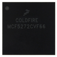
MCF5272CVF66 Freescale Semiconductor, MCF5272CVF66 Datasheet - Page 275

MCF5272CVF66
Manufacturer Part Number
MCF5272CVF66
Description
IC MPU 32BIT 66MHZ 196-MAPBGA
Manufacturer
Freescale Semiconductor
Series
MCF527xr
Specifications of MCF5272CVF66
Core Processor
Coldfire V2
Core Size
32-Bit
Speed
66MHz
Connectivity
EBI/EMI, Ethernet, I²C, SPI, UART/USART, USB
Peripherals
DMA, WDT
Number Of I /o
32
Program Memory Size
16KB (4K x 32)
Program Memory Type
ROM
Ram Size
1K x 32
Voltage - Supply (vcc/vdd)
3 V ~ 3.6 V
Oscillator Type
External
Operating Temperature
-40°C ~ 85°C
Package / Case
196-MAPBGA
Family Name
MCF5xxx
Device Core
ColdFire
Device Core Size
32b
Frequency (max)
66MHz
Instruction Set Architecture
RISC
Supply Voltage 1 (typ)
3.3V
Operating Temp Range
-40C to 85C
Operating Temperature Classification
Industrial
Mounting
Surface Mount
Pin Count
196
Package Type
MA-BGA
Lead Free Status / RoHS Status
Contains lead / RoHS non-compliant
Eeprom Size
-
Data Converters
-
Lead Free Status / Rohs Status
Not Compliant
Available stocks
Company
Part Number
Manufacturer
Quantity
Price
Company:
Part Number:
MCF5272CVF66
Manufacturer:
Freescale Semiconductor
Quantity:
10 000
Part Number:
MCF5272CVF66
Manufacturer:
FREESCALE
Quantity:
20 000
Company:
Part Number:
MCF5272CVF66 K75N
Manufacturer:
ST
Quantity:
18
Company:
Part Number:
MCF5272CVF66J
Manufacturer:
Freescale Semiconductor
Quantity:
10 000
- Current page: 275 of 544
- Download datasheet (7Mb)
12.3.2.13 USB Endpoint 0 Control Register (EP0CTL)
Figure 12-16
specific control (bits 0-9) functions.
Table 12-12
Freescale Semiconductor
31–19
Bits
18
17
16
15
Reset
Reset
Reset
Reset
Field
Field
Field
Field
Addr
R/W
R/W
R/W
R/W
WOR_LVL
WOR_EN
CLK_SEL
DEBUG
lists field descriptions for the USB endpoint 0 control register.
Name
shows the USB endpoint 0 control register. provides both module level and endpoint 0
CRC_ERR
CLK_SEL
—
31
22
15
7
MCF5272 ColdFire
Figure 12-16. USB Endpoint 0 Control Register (EP0CTL)
Reserved, should be cleared.
Debug mode. Enters debug mode. Debug mode enables CRC error generation and notification of
a change of address.
0 Normal operation
1 Enable debug mode functions
Wake-on-ring level select. Selects the active level of INT1 for the wake-on-ring function.
0 Wake-on-ring function is invoked when INT1 pin is 0.
1 Wake-on-ring function is invoked when INT1 pin is 1.
Wake-on-ring enable. Generates a RESUME when the active level is detected on INT1 pin.
0 Wake-on-ring function disabled
1 Wake-on-ring function enabled
Note: the wake-on-ring function generates a RESUME only if the USB module is enabled for
remote wakeup by the host, for example, WAKE_ST = 1, and is suspended.
Clock source selection. Overrides the clock source for the USB module. If the USB_ExtCLK pin is
selected after reset, setting this bit forces the USB module to use the internal system clock.
0 Clock is retrieved from the clock selected at reset.
1 Clock is retrieved from the internal system clock.
Note: the selected clock must have a frequency of 48 MHz.
RESUME
—
14
6
Table 12-12. EP0CTL Field Descriptions
AFE_EN
—
®
13
5
Integrated Microprocessor User’s Manual, Rev. 3
OUT_LVL
BUS_PWR USB_EN CFG_RAM_VAL CMD_ERR CMD_OVER
MBAR + 0x104C
12
4
0000_0000
0000_0000
0000_0000
0000_0000
R/W
R/W
R/W
R/W
—
19
11
3
Description
IN_LVL
DEBUG
18
10
2
WOR_LVL
IN_DONE
17
9
1
Universal Serial Bus (USB)
WOR_EN
—
23
16
8
0
12-17
Related parts for MCF5272CVF66
Image
Part Number
Description
Manufacturer
Datasheet
Request
R
Part Number:
Description:
Mcf5272 Coldfire Integrated Microprocessor User
Manufacturer:
Freescale Semiconductor, Inc
Datasheet:

Part Number:
Description:
MCF5272 Interrupt Service Routine for the Physical Layer Interface Controller
Manufacturer:
Freescale Semiconductor / Motorola
Datasheet:
Part Number:
Description:
Manufacturer:
Freescale Semiconductor, Inc
Datasheet:
Part Number:
Description:
Manufacturer:
Freescale Semiconductor, Inc
Datasheet:
Part Number:
Description:
Manufacturer:
Freescale Semiconductor, Inc
Datasheet:
Part Number:
Description:
Manufacturer:
Freescale Semiconductor, Inc
Datasheet:
Part Number:
Description:
Manufacturer:
Freescale Semiconductor, Inc
Datasheet:
Part Number:
Description:
Manufacturer:
Freescale Semiconductor, Inc
Datasheet:
Part Number:
Description:
Manufacturer:
Freescale Semiconductor, Inc
Datasheet:
Part Number:
Description:
Manufacturer:
Freescale Semiconductor, Inc
Datasheet:
Part Number:
Description:
Manufacturer:
Freescale Semiconductor, Inc
Datasheet:
Part Number:
Description:
Manufacturer:
Freescale Semiconductor, Inc
Datasheet:
Part Number:
Description:
Manufacturer:
Freescale Semiconductor, Inc
Datasheet:
Part Number:
Description:
Manufacturer:
Freescale Semiconductor, Inc
Datasheet:
Part Number:
Description:
Manufacturer:
Freescale Semiconductor, Inc
Datasheet:


