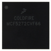
MCF5272CVF66 Freescale Semiconductor, MCF5272CVF66 Datasheet - Page 114

MCF5272CVF66
Manufacturer Part Number
MCF5272CVF66
Description
IC MPU 32BIT 66MHZ 196-MAPBGA
Manufacturer
Freescale Semiconductor
Series
MCF527xr
Specifications of MCF5272CVF66
Core Processor
Coldfire V2
Core Size
32-Bit
Speed
66MHz
Connectivity
EBI/EMI, Ethernet, I²C, SPI, UART/USART, USB
Peripherals
DMA, WDT
Number Of I /o
32
Program Memory Size
16KB (4K x 32)
Program Memory Type
ROM
Ram Size
1K x 32
Voltage - Supply (vcc/vdd)
3 V ~ 3.6 V
Oscillator Type
External
Operating Temperature
-40°C ~ 85°C
Package / Case
196-MAPBGA
Family Name
MCF5xxx
Device Core
ColdFire
Device Core Size
32b
Frequency (max)
66MHz
Instruction Set Architecture
RISC
Supply Voltage 1 (typ)
3.3V
Operating Temp Range
-40C to 85C
Operating Temperature Classification
Industrial
Mounting
Surface Mount
Pin Count
196
Package Type
MA-BGA
Lead Free Status / RoHS Status
Contains lead / RoHS non-compliant
Eeprom Size
-
Data Converters
-
Lead Free Status / Rohs Status
Not Compliant
Available stocks
Company
Part Number
Manufacturer
Quantity
Price
Company:
Part Number:
MCF5272CVF66
Manufacturer:
Freescale Semiconductor
Quantity:
10 000
Part Number:
MCF5272CVF66
Manufacturer:
FREESCALE
Quantity:
20 000
Company:
Part Number:
MCF5272CVF66 K75N
Manufacturer:
ST
Quantity:
18
Company:
Part Number:
MCF5272CVF66J
Manufacturer:
Freescale Semiconductor
Quantity:
10 000
- Current page: 114 of 544
- Download datasheet (7Mb)
Local Memory
4.5.3
Three supervisor registers define the operation of the instruction cache and local bus controller: the cache
control register (CACR) and two access control registers (ACR0, ACR1).
map of the CACR and ACRs. These registers have the following characteristics:
4.5.3.1
The CACR controls operation of the instruction cache. It provides a set of default memory access attributes
for when a reference address does not map into spaces defined by the ACRs. The supervisor-level CACR
is accessed in the CPU address space using the MOVEC instruction with an Rc encoding of 0x002. The
CACR can be read or written when the processor is in background debug mode (BDM).
4-12
•
•
•
•
Reset
Reset
Field CENB
Field
R/W
R/W
Rc
The CACR and ACRs can be accessed only in supervisor mode using the MOVEC instruction with
an Rc value of 0x002 (CACR), 0x004 (ACR0), and 0x005 (ACR1).
Addresses not assigned to the registers and undefined register bits are reserved for future
expansion. Write accesses to these reserved address spaces and reserved register bits have no
effect; read accesses return zeros.
The reset value column indicates the initial value of the register at reset. Uninitialized fields may
contain random values after reset.
The access column indicates whether the corresponding register can be read, written or both.
Attempts to read a write-only register cause zeros to be returned. Attempts to write to a read-only
register are ignored.
31
15
Instruction Cache Programming Model
Cache Control Register (CACR)
Address (using MOVEC) Name Width
30
—
MCF5272 ColdFire
—
29
0x002
0x004
0x005
Table 4-7. Memory Map of Instruction Cache Registers
CDPI CFRZ
28
Figure 4-4. Cache Control Register (CACR)
27
®
CEIB DCM DBWE
CACR
Integrated Microprocessor User’s Manual, Rev. 3
ACR0
ACR1
26
10
Write (R/W by debug module)
Write (R/W by debug module)
—
0000_0000_0000_0000
0000_0000_0000_0000
25
9
32
32
32
CINVA
24
8
0x002
Cache control register
Access control register 0
Access control register 1
23
7
Description
—
6
DWP
5
Table 4-7
4
Reset Value
—
0x0000
0x0000
0x0000
—
Freescale Semiconductor
shows the memory
2
1
CLNF
16
0
Related parts for MCF5272CVF66
Image
Part Number
Description
Manufacturer
Datasheet
Request
R
Part Number:
Description:
Mcf5272 Coldfire Integrated Microprocessor User
Manufacturer:
Freescale Semiconductor, Inc
Datasheet:

Part Number:
Description:
MCF5272 Interrupt Service Routine for the Physical Layer Interface Controller
Manufacturer:
Freescale Semiconductor / Motorola
Datasheet:
Part Number:
Description:
Manufacturer:
Freescale Semiconductor, Inc
Datasheet:
Part Number:
Description:
Manufacturer:
Freescale Semiconductor, Inc
Datasheet:
Part Number:
Description:
Manufacturer:
Freescale Semiconductor, Inc
Datasheet:
Part Number:
Description:
Manufacturer:
Freescale Semiconductor, Inc
Datasheet:
Part Number:
Description:
Manufacturer:
Freescale Semiconductor, Inc
Datasheet:
Part Number:
Description:
Manufacturer:
Freescale Semiconductor, Inc
Datasheet:
Part Number:
Description:
Manufacturer:
Freescale Semiconductor, Inc
Datasheet:
Part Number:
Description:
Manufacturer:
Freescale Semiconductor, Inc
Datasheet:
Part Number:
Description:
Manufacturer:
Freescale Semiconductor, Inc
Datasheet:
Part Number:
Description:
Manufacturer:
Freescale Semiconductor, Inc
Datasheet:
Part Number:
Description:
Manufacturer:
Freescale Semiconductor, Inc
Datasheet:
Part Number:
Description:
Manufacturer:
Freescale Semiconductor, Inc
Datasheet:
Part Number:
Description:
Manufacturer:
Freescale Semiconductor, Inc
Datasheet:


