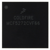
MCF5272CVF66 Freescale Semiconductor, MCF5272CVF66 Datasheet - Page 436

MCF5272CVF66
Manufacturer Part Number
MCF5272CVF66
Description
IC MPU 32BIT 66MHZ 196-MAPBGA
Manufacturer
Freescale Semiconductor
Series
MCF527xr
Specifications of MCF5272CVF66
Core Processor
Coldfire V2
Core Size
32-Bit
Speed
66MHz
Connectivity
EBI/EMI, Ethernet, I²C, SPI, UART/USART, USB
Peripherals
DMA, WDT
Number Of I /o
32
Program Memory Size
16KB (4K x 32)
Program Memory Type
ROM
Ram Size
1K x 32
Voltage - Supply (vcc/vdd)
3 V ~ 3.6 V
Oscillator Type
External
Operating Temperature
-40°C ~ 85°C
Package / Case
196-MAPBGA
Family Name
MCF5xxx
Device Core
ColdFire
Device Core Size
32b
Frequency (max)
66MHz
Instruction Set Architecture
RISC
Supply Voltage 1 (typ)
3.3V
Operating Temp Range
-40C to 85C
Operating Temperature Classification
Industrial
Mounting
Surface Mount
Pin Count
196
Package Type
MA-BGA
Lead Free Status / RoHS Status
Contains lead / RoHS non-compliant
Eeprom Size
-
Data Converters
-
Lead Free Status / Rohs Status
Not Compliant
Available stocks
Company
Part Number
Manufacturer
Quantity
Price
Company:
Part Number:
MCF5272CVF66
Manufacturer:
Freescale Semiconductor
Quantity:
10 000
Part Number:
MCF5272CVF66
Manufacturer:
FREESCALE
Quantity:
20 000
Company:
Part Number:
MCF5272CVF66 K75N
Manufacturer:
ST
Quantity:
18
Company:
Part Number:
MCF5272CVF66J
Manufacturer:
Freescale Semiconductor
Quantity:
10 000
- Current page: 436 of 544
- Download datasheet (7Mb)
Signal Descriptions
19.11.4 USB Transmit Data Negative (USB_TN/PA3)
USB mode: USB_TN is the inverted data transmit output.
Port A mode: This pin can also be configured as the PA3 I/O.
19.11.5 USB Suspend Driver (USB_SUSP/PA4)
USB mode: USB_SUSP is used to put the USB driver in suspend operation.
Port A mode: This pin can also be configured as the PA4 I/O.
19.11.6 USB Transmitter Output Enable (USB_TxEN/PA5)
USB mode: USB_TxEN enables the transceiver to transmit data on the bus. It requires a 4.7-K¾ pullup
resistor to ensure that the external USB Tx driver is off between the MCF5272 coming out of reset and
initializing the port A pin configuration register.
Port A mode: This pin can also be configured as the PA5 I/O.
19.11.7 USB Rx Data Output (USB_RxD/PA6)
USB mode: USB_RxD is the receive data output from the differential receiver inputs USB_RN and
USB_RP.
Port A mode: This pin can also be configured as the PA6 I/O.
19.11.8 USB_D+ and USB_D-
USB_D+ and USB_D- are the on-chip USB interface transceiver signals. When these signals are enabled,
the USB module uses them to communicate to an external USB bus. When not used, each signal should
be pulled to VDD using a 4.7-K¾ resistor.
19.11.9 USB_CLK
USB_CLK is used to connect an external 48-MHz oscillator to the USB module. When this pin is tied to
GND or VDD, the USB module automatically uses the internal CPU clock. In this case the CLKIN must
be 48 MHz if the system is to use the USB function.
19.11.10 INT1/USB Wake-on-Ring (USB_WOR)
The USB module allows for INT1 to generate the USB wake-on-ring signal to the USB host controller.
This function is enabled by a control bit in the USB module. WOR is provided to allow the CPU and the
USB interface to be woken up when in power down mode. This occurs when the USB controller detects a
resume state at the USB inputs.
The interrupt output of an ISDN transceiver, such as the MC145574, can be connected to
INT1/USB_WOR. Before putting the device into sleep mode, the USB module’s wake on ring function
®
MCF5272 ColdFire
Integrated Microprocessor User’s Manual, Rev. 3
19-26
Freescale Semiconductor
Related parts for MCF5272CVF66
Image
Part Number
Description
Manufacturer
Datasheet
Request
R
Part Number:
Description:
Mcf5272 Coldfire Integrated Microprocessor User
Manufacturer:
Freescale Semiconductor, Inc
Datasheet:

Part Number:
Description:
MCF5272 Interrupt Service Routine for the Physical Layer Interface Controller
Manufacturer:
Freescale Semiconductor / Motorola
Datasheet:
Part Number:
Description:
Manufacturer:
Freescale Semiconductor, Inc
Datasheet:
Part Number:
Description:
Manufacturer:
Freescale Semiconductor, Inc
Datasheet:
Part Number:
Description:
Manufacturer:
Freescale Semiconductor, Inc
Datasheet:
Part Number:
Description:
Manufacturer:
Freescale Semiconductor, Inc
Datasheet:
Part Number:
Description:
Manufacturer:
Freescale Semiconductor, Inc
Datasheet:
Part Number:
Description:
Manufacturer:
Freescale Semiconductor, Inc
Datasheet:
Part Number:
Description:
Manufacturer:
Freescale Semiconductor, Inc
Datasheet:
Part Number:
Description:
Manufacturer:
Freescale Semiconductor, Inc
Datasheet:
Part Number:
Description:
Manufacturer:
Freescale Semiconductor, Inc
Datasheet:
Part Number:
Description:
Manufacturer:
Freescale Semiconductor, Inc
Datasheet:
Part Number:
Description:
Manufacturer:
Freescale Semiconductor, Inc
Datasheet:
Part Number:
Description:
Manufacturer:
Freescale Semiconductor, Inc
Datasheet:
Part Number:
Description:
Manufacturer:
Freescale Semiconductor, Inc
Datasheet:


