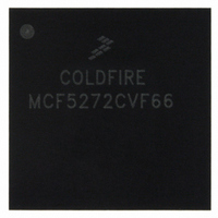
MCF5272CVF66 Freescale Semiconductor, MCF5272CVF66 Datasheet - Page 456

MCF5272CVF66
Manufacturer Part Number
MCF5272CVF66
Description
IC MPU 32BIT 66MHZ 196-MAPBGA
Manufacturer
Freescale Semiconductor
Series
MCF527xr
Specifications of MCF5272CVF66
Core Processor
Coldfire V2
Core Size
32-Bit
Speed
66MHz
Connectivity
EBI/EMI, Ethernet, I²C, SPI, UART/USART, USB
Peripherals
DMA, WDT
Number Of I /o
32
Program Memory Size
16KB (4K x 32)
Program Memory Type
ROM
Ram Size
1K x 32
Voltage - Supply (vcc/vdd)
3 V ~ 3.6 V
Oscillator Type
External
Operating Temperature
-40°C ~ 85°C
Package / Case
196-MAPBGA
Family Name
MCF5xxx
Device Core
ColdFire
Device Core Size
32b
Frequency (max)
66MHz
Instruction Set Architecture
RISC
Supply Voltage 1 (typ)
3.3V
Operating Temp Range
-40C to 85C
Operating Temperature Classification
Industrial
Mounting
Surface Mount
Pin Count
196
Package Type
MA-BGA
Lead Free Status / RoHS Status
Contains lead / RoHS non-compliant
Eeprom Size
-
Data Converters
-
Lead Free Status / Rohs Status
Not Compliant
Available stocks
Company
Part Number
Manufacturer
Quantity
Price
Company:
Part Number:
MCF5272CVF66
Manufacturer:
Freescale Semiconductor
Quantity:
10 000
Part Number:
MCF5272CVF66
Manufacturer:
FREESCALE
Quantity:
20 000
Company:
Part Number:
MCF5272CVF66 K75N
Manufacturer:
ST
Quantity:
18
Company:
Part Number:
MCF5272CVF66J
Manufacturer:
Freescale Semiconductor
Quantity:
10 000
- Current page: 456 of 544
- Download datasheet (7Mb)
Bus Operation
20.6.1
CSBRn[EBI] is 00 for FLASH/SRAM devices and peripherals having 16- or 32-bit data bus widths. These
memory devices have separate pins for independent byte strobes, write enable, chip select, and output
enable. All chip selects support this EBI mode.
The number of wait states required for the external memory or peripheral is programmed through
CSORn[WS]. The external transfer acknowledge signal, TA, is provided to allow off-chip control of wait
states. External control of wait states is enabled when CSORn[WS] is 0x1F. When TA is used to terminate
the bus cycle, the bus cycle will have a minimum of one wait states. Additional wait states can be added
by delaying the assertion of TA.
20-8
SRAM/ROM
SRAM/ROM
16-/32-bit
Reserved
SDRAM
8-bit
A0
SDCLK
A[22:0]
D[31:0]
OE, BS[3:0]
R/W
CSn
TA
Interface for FLASH/SRAM Devices with Byte Strobes
CSBRn[EBI]
Wait states, if needed, are added immediately after C2 in
Figure 20-3. Longword Read; EBI = 00; 32-Bit Port; Internal Termination
(H)
(H)
00
01
10
11
MCF5272 ColdFire
Table 20-7. External Bus Interface Codes for CSBRs
Applicable Chip Select
CS7/SDCS only
All
All
—
®
Integrated Microprocessor User’s Manual, Rev. 3
C1
NOTE
For 16/32 bit wide memory devices with byte strobe inputs.
are byte read/write enables in this mode. CSBR0[EBI] = 00 at
reset.
One physical bank of SDRAM consisting of 16–256 Mbit devices.
The CS7/SDCS CSORn[WS] must be set to 0x1F.
—
SRAM/ROM timing for 8 bit wide memory devices without byte
strobe inputs.
BS[3:0]
C2
function as byte write enables in this mode.
Figure
Note
20-3.
Freescale Semiconductor
BS[3:0]
Related parts for MCF5272CVF66
Image
Part Number
Description
Manufacturer
Datasheet
Request
R
Part Number:
Description:
Mcf5272 Coldfire Integrated Microprocessor User
Manufacturer:
Freescale Semiconductor, Inc
Datasheet:

Part Number:
Description:
MCF5272 Interrupt Service Routine for the Physical Layer Interface Controller
Manufacturer:
Freescale Semiconductor / Motorola
Datasheet:
Part Number:
Description:
Manufacturer:
Freescale Semiconductor, Inc
Datasheet:
Part Number:
Description:
Manufacturer:
Freescale Semiconductor, Inc
Datasheet:
Part Number:
Description:
Manufacturer:
Freescale Semiconductor, Inc
Datasheet:
Part Number:
Description:
Manufacturer:
Freescale Semiconductor, Inc
Datasheet:
Part Number:
Description:
Manufacturer:
Freescale Semiconductor, Inc
Datasheet:
Part Number:
Description:
Manufacturer:
Freescale Semiconductor, Inc
Datasheet:
Part Number:
Description:
Manufacturer:
Freescale Semiconductor, Inc
Datasheet:
Part Number:
Description:
Manufacturer:
Freescale Semiconductor, Inc
Datasheet:
Part Number:
Description:
Manufacturer:
Freescale Semiconductor, Inc
Datasheet:
Part Number:
Description:
Manufacturer:
Freescale Semiconductor, Inc
Datasheet:
Part Number:
Description:
Manufacturer:
Freescale Semiconductor, Inc
Datasheet:
Part Number:
Description:
Manufacturer:
Freescale Semiconductor, Inc
Datasheet:
Part Number:
Description:
Manufacturer:
Freescale Semiconductor, Inc
Datasheet:


