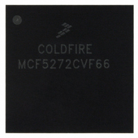
MCF5272CVF66 Freescale Semiconductor, MCF5272CVF66 Datasheet - Page 445

MCF5272CVF66
Manufacturer Part Number
MCF5272CVF66
Description
IC MPU 32BIT 66MHZ 196-MAPBGA
Manufacturer
Freescale Semiconductor
Series
MCF527xr
Specifications of MCF5272CVF66
Core Processor
Coldfire V2
Core Size
32-Bit
Speed
66MHz
Connectivity
EBI/EMI, Ethernet, I²C, SPI, UART/USART, USB
Peripherals
DMA, WDT
Number Of I /o
32
Program Memory Size
16KB (4K x 32)
Program Memory Type
ROM
Ram Size
1K x 32
Voltage - Supply (vcc/vdd)
3 V ~ 3.6 V
Oscillator Type
External
Operating Temperature
-40°C ~ 85°C
Package / Case
196-MAPBGA
Family Name
MCF5xxx
Device Core
ColdFire
Device Core Size
32b
Frequency (max)
66MHz
Instruction Set Architecture
RISC
Supply Voltage 1 (typ)
3.3V
Operating Temp Range
-40C to 85C
Operating Temperature Classification
Industrial
Mounting
Surface Mount
Pin Count
196
Package Type
MA-BGA
Lead Free Status / RoHS Status
Contains lead / RoHS non-compliant
Eeprom Size
-
Data Converters
-
Lead Free Status / Rohs Status
Not Compliant
Available stocks
Company
Part Number
Manufacturer
Quantity
Price
Company:
Part Number:
MCF5272CVF66
Manufacturer:
Freescale Semiconductor
Quantity:
10 000
Part Number:
MCF5272CVF66
Manufacturer:
FREESCALE
Quantity:
20 000
Company:
Part Number:
MCF5272CVF66 K75N
Manufacturer:
ST
Quantity:
18
Company:
Part Number:
MCF5272CVF66J
Manufacturer:
Freescale Semiconductor
Quantity:
10 000
- Current page: 445 of 544
- Download datasheet (7Mb)
Signal Descriptions
GCI mode: This pin can be configured as a dedicated output for clocking data out of GCI port 3. Data is
clocked out of DOUT3 on the rising edge of DCL1. DCL1 is twice the bit rate, that is, two clocks per data
bit. This is done by setting a bit in the PLIC module configuration register this pin can be configured as a
dedicated output for IDL/GCI port 3.
Port A mode: I/O pin PA7.
19.16.3.4 INT4 and Port 3 GCI/IDL Data In (INT4/DIN3)
IDL mode: This pin can be configured as a dedicated input, DIN3, for clocking data into IDL port 3. Data
is clocked into DIN3 on the falling edge of DCL1. Data is clocked into DIN3 on the falling edge of DCL1.
This is done by setting a bit in the PLIC module configuration register. Note that the appropriate bits must
be set in the pin configuration register to reassign this pin from the interrupt module to the PLIC module.
GCI mode: This pin can be configured as a dedicated input, DIN3, for clocking data into GCI port 3. DCL1
is twice the bit rate, that is, two clocks per data bit. This is done by setting a bit in the PLIC module
configuration register. Note that the appropriate bits must be set in the pin configuration register to reassign
this spin from the interrupt module to the PLIC module.
Interrupt mode: This signal can be configured as interrupt input 4.
19.17 JTAG Test Access Port and BDM Debug Port
The MCF5272 supports the Freescale background debug mode (BDM) for ColdFire processors. It also
supports a JTAG test interface.
The following signals do not support JTAG due to the critical timing required to support SDRAM memory:
BS[3:0], RAS0, CAS0, SDCLK, SDCLKE, SDRAMCS/CS7, SDWE, A10_PRECHG, SDBA[1:0],
D[31:0], A[15:0].
19.17.1 Test Clock (TCK/PSTCLK)
JTAG mode: TCK is the dedicated JTAG test logic clock, independent of the CPU system clock. This input
provides a clock for on-board test logic defined by the IEEE 1149.1 standard.
TCK should be grounded if the JTAG port is not used and MTMOD is tied low.
BDM mode: PSTCLK is an output at the same frequency as the CPU clock. It is used for indicating valid
processor status data on the PST and DDATA pins.
19.17.2 Test Mode Select and Force Breakpoint (TMS/BKPT)
JTAG mode: The TMS input controls test mode operations for on-board test logic defined by the IEEE
1149.1 standard. Connecting TMS to VDD disables the test controller, making all JTAG circuits
transparent to the system.
BDM mode: The hardware breakpoint input, BKPT, requires a 10-K¾ pullup resistor.
®
MCF5272 ColdFire
Integrated Microprocessor User’s Manual, Rev. 3
Freescale Semiconductor
19-35
Related parts for MCF5272CVF66
Image
Part Number
Description
Manufacturer
Datasheet
Request
R
Part Number:
Description:
Mcf5272 Coldfire Integrated Microprocessor User
Manufacturer:
Freescale Semiconductor, Inc
Datasheet:

Part Number:
Description:
MCF5272 Interrupt Service Routine for the Physical Layer Interface Controller
Manufacturer:
Freescale Semiconductor / Motorola
Datasheet:
Part Number:
Description:
Manufacturer:
Freescale Semiconductor, Inc
Datasheet:
Part Number:
Description:
Manufacturer:
Freescale Semiconductor, Inc
Datasheet:
Part Number:
Description:
Manufacturer:
Freescale Semiconductor, Inc
Datasheet:
Part Number:
Description:
Manufacturer:
Freescale Semiconductor, Inc
Datasheet:
Part Number:
Description:
Manufacturer:
Freescale Semiconductor, Inc
Datasheet:
Part Number:
Description:
Manufacturer:
Freescale Semiconductor, Inc
Datasheet:
Part Number:
Description:
Manufacturer:
Freescale Semiconductor, Inc
Datasheet:
Part Number:
Description:
Manufacturer:
Freescale Semiconductor, Inc
Datasheet:
Part Number:
Description:
Manufacturer:
Freescale Semiconductor, Inc
Datasheet:
Part Number:
Description:
Manufacturer:
Freescale Semiconductor, Inc
Datasheet:
Part Number:
Description:
Manufacturer:
Freescale Semiconductor, Inc
Datasheet:
Part Number:
Description:
Manufacturer:
Freescale Semiconductor, Inc
Datasheet:
Part Number:
Description:
Manufacturer:
Freescale Semiconductor, Inc
Datasheet:


