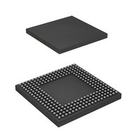
HD6417727BP100BV Renesas Electronics America, HD6417727BP100BV Datasheet - Page 368

HD6417727BP100BV
Manufacturer Part Number
HD6417727BP100BV
Description
IC SUPERH MPU ROMLESS 240BGA
Manufacturer
Renesas Electronics America
Series
SuperH® SH7700r
Datasheet
1.HD6417727BP100CV.pdf
(1098 pages)
Specifications of HD6417727BP100BV
Core Processor
SH-3 DSP
Core Size
32-Bit
Speed
100MHz
Connectivity
FIFO, SCI, SIO, SmartCard, USB
Peripherals
DMA, LCD, POR, WDT
Number Of I /o
104
Program Memory Type
ROMless
Ram Size
32K x 8
Voltage - Supply (vcc/vdd)
1.6 V ~ 2.05 V
Data Converters
A/D 6x10b; D/A 2x8b
Oscillator Type
Internal
Operating Temperature
-20°C ~ 75°C
Package / Case
240-BGA
Lead Free Status / RoHS Status
Contains lead / RoHS non-compliant
Eeprom Size
-
Program Memory Size
-
- Current page: 368 of 1098
- Download datasheet (7Mb)
Section 12 Bus State Controller (BSC)
12.2.7
The synchronous DRAM mode register (SDMR) is written to via the synchronous DRAM address
bus and is an 8-bit write-only register. It sets synchronous DRAM mode for areas 2 and 3. SDMR
is undefined after a power-on reset. The register contents are not initialized by a manual reset or
standby mode; values remain unchanged.
Note: * Depending on the type of synchronous DRAM.
Writes to the synchronous DRAM mode register use the address bus rather than the data bus. If
the value to be set is X and the SDMR address is Y, the value X is written in the synchronous
DRAM mode register by writing in address X + Y. Since, with a 32-bit bus width, A0 of the
synchronous DRAM is connected to A2 of the chip and A1 of the synchronous DRAM is
connected to A3 of the chip, the value actually written to the synchronous DRAM is the X value
shifted two bits right. With a 16-bit bus width, the value written is the X value shifted one bit
right. For example, with a 32-bit bus width, when H'0230 is written to the SDMR register of area
2, random data is written to the address H'FFFFD000 (address Y) + H'08C0 (value X), or
H'FFFFD8C0. As a result, H'0230 is written to the SDMR register. The range for value X is
H'0000 to H'0FFC. When H'0230 is written to the SDMR register of area 3, random data is written
to the address H'FFFFE000 (address Y) + H'08C0 (value X), or H'FFFFE8C0. As a result, H'0230
is written to the SDMR register. The range for value X is H'0000 to H'0FFC.
Rev.6.00 Mar. 27, 2009 Page 310 of 1036
REJ09B0254-0600
Initial value:
R/W:
Bit:
Synchronous DRAM Mode Register (SDMR)
31
—
—
SDMR address
......................
......................
......................
12
—
—
W*
11
—
—
W*
10
—
—
—
—
W
9
—
—
W
8
—
—
W
7
—
—
W
6
—
—
W
5
—
—
W
4
—
—
W
3
—
—
W
2
—
—
—
1
—
—
—
0
Related parts for HD6417727BP100BV
Image
Part Number
Description
Manufacturer
Datasheet
Request
R

Part Number:
Description:
KIT STARTER FOR M16C/29
Manufacturer:
Renesas Electronics America
Datasheet:

Part Number:
Description:
KIT STARTER FOR R8C/2D
Manufacturer:
Renesas Electronics America
Datasheet:

Part Number:
Description:
R0K33062P STARTER KIT
Manufacturer:
Renesas Electronics America
Datasheet:

Part Number:
Description:
KIT STARTER FOR R8C/23 E8A
Manufacturer:
Renesas Electronics America
Datasheet:

Part Number:
Description:
KIT STARTER FOR R8C/25
Manufacturer:
Renesas Electronics America
Datasheet:

Part Number:
Description:
KIT STARTER H8S2456 SHARPE DSPLY
Manufacturer:
Renesas Electronics America
Datasheet:

Part Number:
Description:
KIT STARTER FOR R8C38C
Manufacturer:
Renesas Electronics America
Datasheet:

Part Number:
Description:
KIT STARTER FOR R8C35C
Manufacturer:
Renesas Electronics America
Datasheet:

Part Number:
Description:
KIT STARTER FOR R8CL3AC+LCD APPS
Manufacturer:
Renesas Electronics America
Datasheet:

Part Number:
Description:
KIT STARTER FOR RX610
Manufacturer:
Renesas Electronics America
Datasheet:

Part Number:
Description:
KIT STARTER FOR R32C/118
Manufacturer:
Renesas Electronics America
Datasheet:

Part Number:
Description:
KIT DEV RSK-R8C/26-29
Manufacturer:
Renesas Electronics America
Datasheet:

Part Number:
Description:
KIT STARTER FOR SH7124
Manufacturer:
Renesas Electronics America
Datasheet:

Part Number:
Description:
KIT STARTER FOR H8SX/1622
Manufacturer:
Renesas Electronics America
Datasheet:

Part Number:
Description:
KIT DEV FOR SH7203
Manufacturer:
Renesas Electronics America
Datasheet:


