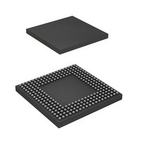
HD6417727BP100BV Renesas Electronics America, HD6417727BP100BV Datasheet - Page 344

HD6417727BP100BV
Manufacturer Part Number
HD6417727BP100BV
Description
IC SUPERH MPU ROMLESS 240BGA
Manufacturer
Renesas Electronics America
Series
SuperH® SH7700r
Datasheet
1.HD6417727BP100CV.pdf
(1098 pages)
Specifications of HD6417727BP100BV
Core Processor
SH-3 DSP
Core Size
32-Bit
Speed
100MHz
Connectivity
FIFO, SCI, SIO, SmartCard, USB
Peripherals
DMA, LCD, POR, WDT
Number Of I /o
104
Program Memory Type
ROMless
Ram Size
32K x 8
Voltage - Supply (vcc/vdd)
1.6 V ~ 2.05 V
Data Converters
A/D 6x10b; D/A 2x8b
Oscillator Type
Internal
Operating Temperature
-20°C ~ 75°C
Package / Case
240-BGA
Lead Free Status / RoHS Status
Contains lead / RoHS non-compliant
Eeprom Size
-
Program Memory Size
-
- Current page: 344 of 1098
- Download datasheet (7Mb)
Section 12 Bus State Controller (BSC)
12.1.3
Table 12.1 lists the BSC pin configuration.
Table 12.1 Pin Configuration
Pin Name
Address bus
Data bus
Bus cycle start
Chip select 0, 2–4
Chip select 5, 6
PCMCIA card select
Read/write
Row address strobe
Column address strobe
Data enable 0
Data enable 1
Data enable 2
Rev.6.00 Mar. 27, 2009 Page 286 of 1036
REJ09B0254-0600
Pin Configuration
A25–A0
D31–D16
BS
CS0, CS2–CS4
CS5/CE1A,
CS6/CE1B
CE2A, CE2B
RD/WR
RAS
CAS
WE0/DQMLL
WE1/DQMLU/
WE
WE2/DQMUL/
ICIORD
Signal
D15–D0
I/O
Output
I/O
Output
Output
Output
Output
Output
Output
Output
Output
Output
Output
I/O
Description
Address output
When 32-bit bus width, data I/O
Shows start of bus cycle. During burst
transfers, asserts every data cycle.
Chip select signal to indicate area being
accessed.
Chip select signal to indicate area being
accessed. CS5/CE1A and CS6/CE1B can
also be used as CE1A and CE1B of
PCMCIA.
When PCMCIA is used, CE2A and CE2B
Data bus direction indicator signal.
PCMCIA write indicator signal.
When synchronous DRAM is used, RAS
signal.
When synchronous DRAM is used, CAS
signal.
When memory other than synchronous
DRAM is used, selects D7 to D0 write
strobe signal. When synchronous DRAM is
used, selects D7 to D0.
When memory other than synchronous
DRAM and PCMCIA is used, selects D15
to D8 write strobe signal. When
synchronous DRAM is used, selects D15 to
D8. When PCMCIA is used, strobe signal
that indicates the write cycle.
When memory other than synchronous
DRAM and PCMCIA is used, selects D23
to D16 write strobe signal. When
synchronous DRAM is used, selects D23 to
D16. When PCMCIA is used, strobe signal
indicating I/O read.
Data I/O
Related parts for HD6417727BP100BV
Image
Part Number
Description
Manufacturer
Datasheet
Request
R

Part Number:
Description:
KIT STARTER FOR M16C/29
Manufacturer:
Renesas Electronics America
Datasheet:

Part Number:
Description:
KIT STARTER FOR R8C/2D
Manufacturer:
Renesas Electronics America
Datasheet:

Part Number:
Description:
R0K33062P STARTER KIT
Manufacturer:
Renesas Electronics America
Datasheet:

Part Number:
Description:
KIT STARTER FOR R8C/23 E8A
Manufacturer:
Renesas Electronics America
Datasheet:

Part Number:
Description:
KIT STARTER FOR R8C/25
Manufacturer:
Renesas Electronics America
Datasheet:

Part Number:
Description:
KIT STARTER H8S2456 SHARPE DSPLY
Manufacturer:
Renesas Electronics America
Datasheet:

Part Number:
Description:
KIT STARTER FOR R8C38C
Manufacturer:
Renesas Electronics America
Datasheet:

Part Number:
Description:
KIT STARTER FOR R8C35C
Manufacturer:
Renesas Electronics America
Datasheet:

Part Number:
Description:
KIT STARTER FOR R8CL3AC+LCD APPS
Manufacturer:
Renesas Electronics America
Datasheet:

Part Number:
Description:
KIT STARTER FOR RX610
Manufacturer:
Renesas Electronics America
Datasheet:

Part Number:
Description:
KIT STARTER FOR R32C/118
Manufacturer:
Renesas Electronics America
Datasheet:

Part Number:
Description:
KIT DEV RSK-R8C/26-29
Manufacturer:
Renesas Electronics America
Datasheet:

Part Number:
Description:
KIT STARTER FOR SH7124
Manufacturer:
Renesas Electronics America
Datasheet:

Part Number:
Description:
KIT STARTER FOR H8SX/1622
Manufacturer:
Renesas Electronics America
Datasheet:

Part Number:
Description:
KIT DEV FOR SH7203
Manufacturer:
Renesas Electronics America
Datasheet:


