M306N4FGGP#U3 Renesas Electronics America, M306N4FGGP#U3 Datasheet - Page 405
M306N4FGGP#U3
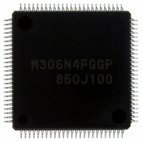
Manufacturer Part Number
M306N4FGGP#U3
Description
IC M16C/6N4 MCU FLASH 100-LQFP
Manufacturer
Renesas Electronics America
Series
M16C™ M16C/6Nr
Specifications of M306N4FGGP#U3
Core Processor
M16C/60
Core Size
16-Bit
Speed
24MHz
Connectivity
CAN, I²C, IEBus, SIO, UART/USART
Peripherals
DMA, WDT
Number Of I /o
85
Program Memory Size
256KB (256K x 8)
Program Memory Type
FLASH
Ram Size
10K x 8
Voltage - Supply (vcc/vdd)
3 V ~ 5.5 V
Data Converters
A/D 26x10b; D/A 2x8b
Oscillator Type
Internal
Operating Temperature
-40°C ~ 85°C
Package / Case
100-LQFP
Package
100LQFP
Family Name
M16C
Maximum Speed
24 MHz
Operating Supply Voltage
3.3|5 V
Data Bus Width
16|32 Bit
Number Of Programmable I/os
87
Interface Type
I2C/UART
On-chip Adc
26-chx10-bit
On-chip Dac
2-chx8-bit
Number Of Timers
11
For Use With
R0K3306NKS001BE - KIT DEV RSK RSK-M16C/6NKR0K3306NKS000BE - KIT DEV RSK RSK-M16C/6NK
Lead Free Status / RoHS Status
Lead free / RoHS Compliant
Eeprom Size
-
Available stocks
Company
Part Number
Manufacturer
Quantity
Price


2.00 Nov. 10, 2004
Rev.
Date
REVISION HISTORY
Page
219
223
224
225
231
233
234
251
252
255
256
257
258
260
261
262
265
266
271
273
274
276
Figure 19.8 C0STR and C1STR Registers (upper): NOTE 2 is added.
19.5 Operational Modes
Figure 19.12 Transition Between Operational Modes is revised.
19.5.1 CAN Reset/Initialization Mode is revised.
19.5.2 CAN Operation Mode is revised.
19.5.3 CAN Sleep Mode is revised.
19.5.4 CAN Interface Sleep Mode is added.
19.5.5 Bus Off State is revised.
19.12 Return from Bus Off Function is revised.
19.14 Listen-Only Mode
Figure 19.20 Timing of Receive Data Frame Sequence: Waveform of RecState bit is revised.
19.15.1 Reception: (4) (5) are revised.
Figure 19.21 Timing of Transmit Sequence
19.15.2 Transmission: (1) to (4) are revised.
21.2.1 ROM Code Protect Function is revised.
21.2.2 ID Code Check Function is revised.
Figure 21.2 ROMCP Register is revised.
Figure 21.4 (upper) FMR0 Register: The value of After Reset is revised.
21.3.3.1 FMR00 Bit is revised.
21.3.3.8 FMR11 Bit is revised.
21.3.3.9 FMR16 Bit is revised.
Figure 21.5 Setting and Resetting of EW0 Mode is revised.
Figure 21.6 Setting and Resetting of EW1 Mode: NOTE 3 is revised.
Figure 21.7 Processing Before and After Low Power Dissipation Mode: NOTE 4 is added.
21.3.4.12 Low Power Dissipation Mode and On-chip Oscillator Low Power Dissipation
Mode is revised.
Table 21.4 Software Commands: NOTE 2 is deleted.
21.3.5.4 Program Command (40h)
Figure 21.11 Read Lock Bit Status Command
21.3.7.1 Sequencer Status (SR7 and FMR00 Bits) is revised.
Table 21.7 Pin Functions for Standard Serial I/O Mode
Figure 21.14 Pin Connections for Standard Serial I/O Mode (2) is added.
Figure 21.16 Circuit Application in Standard Serial I/O Mode 2: "RESET" is added.
Table 21.8 Pin Functions for CAN I/O Mode
• 1st line: "three operational modes" is revised to "four operational modes".
• 5th line: "CAN Interface Sleep Mode" is added.
• last line: "When listen-only mode is selected, do not request the transmission." is added.
• The position of the number corresponding to the text is revised.
• From bottom to 3rd line: "read command" is revised to "read array command".
• "Locked", "Not locked" are revised to "Block is locked", "Block is not locked".
• "VCC" is revised to "VCC1", and "VCC2" is added.
• VCC1, VCC2, VSS: VCC apply condition is added.
• "VCC" is revised to "VCC1", and "VCC2" is added.
• VCC1, VCC2, VSS: VCC apply condition is added.
M16C/6N Group (M16C/6N4) Hardware Manual
C-5
Description
Summary
____________
Related parts for M306N4FGGP#U3
Image
Part Number
Description
Manufacturer
Datasheet
Request
R

Part Number:
Description:
KIT STARTER FOR M16C/29
Manufacturer:
Renesas Electronics America
Datasheet:

Part Number:
Description:
KIT STARTER FOR R8C/2D
Manufacturer:
Renesas Electronics America
Datasheet:

Part Number:
Description:
R0K33062P STARTER KIT
Manufacturer:
Renesas Electronics America
Datasheet:

Part Number:
Description:
KIT STARTER FOR R8C/23 E8A
Manufacturer:
Renesas Electronics America
Datasheet:

Part Number:
Description:
KIT STARTER FOR R8C/25
Manufacturer:
Renesas Electronics America
Datasheet:

Part Number:
Description:
KIT STARTER H8S2456 SHARPE DSPLY
Manufacturer:
Renesas Electronics America
Datasheet:

Part Number:
Description:
KIT STARTER FOR R8C38C
Manufacturer:
Renesas Electronics America
Datasheet:

Part Number:
Description:
KIT STARTER FOR R8C35C
Manufacturer:
Renesas Electronics America
Datasheet:

Part Number:
Description:
KIT STARTER FOR R8CL3AC+LCD APPS
Manufacturer:
Renesas Electronics America
Datasheet:
Part Number:
Description:
KIT STARTER FOR RX610
Manufacturer:
Renesas Electronics America
Datasheet:

Part Number:
Description:
KIT STARTER FOR R32C/118
Manufacturer:
Renesas Electronics America
Datasheet:

Part Number:
Description:
KIT DEV RSK-R8C/26-29
Manufacturer:
Renesas Electronics America
Datasheet:

Part Number:
Description:
KIT STARTER FOR SH7124
Manufacturer:
Renesas Electronics America
Datasheet:

Part Number:
Description:
KIT STARTER FOR H8SX/1622
Manufacturer:
Renesas Electronics America
Datasheet:

Part Number:
Description:
KIT DEV FOR SH7203
Manufacturer:
Renesas Electronics America
Datasheet: