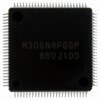
M306N4FGGP#U3 Renesas Electronics America, M306N4FGGP#U3 Datasheet - Page 271

M306N4FGGP#U3
Manufacturer Part Number
M306N4FGGP#U3
Description
IC M16C/6N4 MCU FLASH 100-LQFP
Manufacturer
Renesas Electronics America
Series
M16C™ M16C/6Nr
Specifications of M306N4FGGP#U3
Core Processor
M16C/60
Core Size
16-Bit
Speed
24MHz
Connectivity
CAN, I²C, IEBus, SIO, UART/USART
Peripherals
DMA, WDT
Number Of I /o
85
Program Memory Size
256KB (256K x 8)
Program Memory Type
FLASH
Ram Size
10K x 8
Voltage - Supply (vcc/vdd)
3 V ~ 5.5 V
Data Converters
A/D 26x10b; D/A 2x8b
Oscillator Type
Internal
Operating Temperature
-40°C ~ 85°C
Package / Case
100-LQFP
Package
100LQFP
Family Name
M16C
Maximum Speed
24 MHz
Operating Supply Voltage
3.3|5 V
Data Bus Width
16|32 Bit
Number Of Programmable I/os
87
Interface Type
I2C/UART
On-chip Adc
26-chx10-bit
On-chip Dac
2-chx8-bit
Number Of Timers
11
For Use With
R0K3306NKS001BE - KIT DEV RSK RSK-M16C/6NKR0K3306NKS000BE - KIT DEV RSK RSK-M16C/6NK
Lead Free Status / RoHS Status
Lead free / RoHS Compliant
Eeprom Size
-
Available stocks
Company
Part Number
Manufacturer
Quantity
Price
- Current page: 271 of 414
- Download datasheet (3Mb)
M16C/6N Group (M16C/6N4)
Rev.2.40
REJ09B0009-0240
Figure 20.9 Registers PUR0, PUR1, and PUR2
Apr 14, 2006
Pull-up Control Register 0
Pull-up Control Register 1
NOTES:
Pull-up Control Register 2
NOTES:
NOTES:
b7
b7
b7
1. The values after hardware reset is as follows:
2. During memory expansion and microprocessor modes, the pins are not pulled high although the contents of
3. If bits PM01 to PM00 are set to 01b (memory expansion mode) or 11b (microprocessor mode) in a program
4. The P7_1 pin does not have pull-up.
5. The pin for which this bit is 1 (pulled high) and the direction bit is 0 (input mode) is pulled high.
1. The P8_5 pin does not have pull-up.
2. The P9_1 pin does not have pull-up.
3. The pin for which this bit is 1 (pulled high) and the direction bit is 0 (input mode) is pulled high.
1. During memory expansion and microprocessor modes, the pins are not pulled high although their corresponding
2. The pin for which this bit is 1 (pulled high) and the direction bit is 0 (input mode) is pulled high.
b6
b6
b6
The values after software reset, watchdog timer reset and oscillation stop detection reset are as follows:
these bits can be modified.
during single-chip mode, the PU11 bit becomes 1.
register contents can be modified.
00000000b when input on CNVSS pin is "L".
00000010b when input on CNVSS pin is "H".
00000000b when bits PM 01 to PM00 in the PM0 register are 00b (single-chip mode).
00000010b when bits PM 01 to PM00 are 01b (memory expansion mode) or 11b (microprocessor mode).
b5
b5
b5
b4
b4
b4
page 247 of 376
b3
b3
b3
b2
b2
b2
b1
b1
b1
b0
b0
b0
Bit Symbol
Bit Symbol
Bit Symbol
(b7-b6)
PU00
PU01
PU02
PU03
PU04
PU05
PU06
PU07
PU10
PU11
PU12
PU13
PU14
PU15
PU16
PU17
PU20
PU21
PU22
PU23
PU24
PU25
-
(1)
Symbol
Symbol
Symbol
PUR0
PUR1
PUR2
P0_0 to P0_3 pull-up
P0_4 to P0_7 pull-up
P1_0 to P1_3 pull-up
P1_4 to P1_7 pull-up
P2_0 to P2_3 pull-up
P2_4 to P2_7 pull-up
P3_0 to P3_3 pull-up
P3_4 to P3_7 pull-up
P4_0 to P4_3 pull-up
P4_4 to P4_7 pull-up
P5_0 to P5_3 pull-up
P5_4 to P5_7 pull-up
P6_0 to P6_3 pull-up
P6_4 to P6_7 pull-up
P7_0, P7_2, and P7_3 pull-up
P7_4 to P7_7 pull-up
P8_0 to P8_3 pull-up
P8_4, P8_6, and P8_7 pull-up
P9_0, P9_2, and P9_3 pull-up
P9_4 to P9_7 pull-up
P10_0 to P10_3 pull-up
P10_4 to P10_7 pull-up
Nothing is assigned. If necessary, set to 0.
When read, the content is 0.
Bit Name
Bit Name
Bit Name
(2)
(3)
(2)
(2)
Address
Address
Address
03FCh
03FDh
03FEh
(4)
(1)
(2)
0 : Not pulled high
1 : Pulled high
0 : Not pulled high
1 : Pulled high
0 : Not pulled high
1 : Pulled high
Function
Function
Function
After Reset
00000000b
00000010b
After Reset
After Reset
20. Programmable I/O Ports
(2)
(5)
(3)
00h
00h
(1)
RW
RW
RW
RW
RW
RW
RW
RW
RW
RW
RW
RW
RW
RW
RW
RW
RW
RW
RW
RW
RW
RW
RW
RW
RW
-
Related parts for M306N4FGGP#U3
Image
Part Number
Description
Manufacturer
Datasheet
Request
R

Part Number:
Description:
KIT STARTER FOR M16C/29
Manufacturer:
Renesas Electronics America
Datasheet:

Part Number:
Description:
KIT STARTER FOR R8C/2D
Manufacturer:
Renesas Electronics America
Datasheet:

Part Number:
Description:
R0K33062P STARTER KIT
Manufacturer:
Renesas Electronics America
Datasheet:

Part Number:
Description:
KIT STARTER FOR R8C/23 E8A
Manufacturer:
Renesas Electronics America
Datasheet:

Part Number:
Description:
KIT STARTER FOR R8C/25
Manufacturer:
Renesas Electronics America
Datasheet:

Part Number:
Description:
KIT STARTER H8S2456 SHARPE DSPLY
Manufacturer:
Renesas Electronics America
Datasheet:

Part Number:
Description:
KIT STARTER FOR R8C38C
Manufacturer:
Renesas Electronics America
Datasheet:

Part Number:
Description:
KIT STARTER FOR R8C35C
Manufacturer:
Renesas Electronics America
Datasheet:

Part Number:
Description:
KIT STARTER FOR R8CL3AC+LCD APPS
Manufacturer:
Renesas Electronics America
Datasheet:

Part Number:
Description:
KIT STARTER FOR RX610
Manufacturer:
Renesas Electronics America
Datasheet:

Part Number:
Description:
KIT STARTER FOR R32C/118
Manufacturer:
Renesas Electronics America
Datasheet:

Part Number:
Description:
KIT DEV RSK-R8C/26-29
Manufacturer:
Renesas Electronics America
Datasheet:

Part Number:
Description:
KIT STARTER FOR SH7124
Manufacturer:
Renesas Electronics America
Datasheet:

Part Number:
Description:
KIT STARTER FOR H8SX/1622
Manufacturer:
Renesas Electronics America
Datasheet:

Part Number:
Description:
KIT DEV FOR SH7203
Manufacturer:
Renesas Electronics America
Datasheet:


