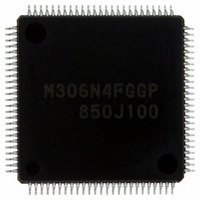
M306N4FGGP#U3 Renesas Electronics America, M306N4FGGP#U3 Datasheet - Page 286

M306N4FGGP#U3
Manufacturer Part Number
M306N4FGGP#U3
Description
IC M16C/6N4 MCU FLASH 100-LQFP
Manufacturer
Renesas Electronics America
Series
M16C™ M16C/6Nr
Specifications of M306N4FGGP#U3
Core Processor
M16C/60
Core Size
16-Bit
Speed
24MHz
Connectivity
CAN, I²C, IEBus, SIO, UART/USART
Peripherals
DMA, WDT
Number Of I /o
85
Program Memory Size
256KB (256K x 8)
Program Memory Type
FLASH
Ram Size
10K x 8
Voltage - Supply (vcc/vdd)
3 V ~ 5.5 V
Data Converters
A/D 26x10b; D/A 2x8b
Oscillator Type
Internal
Operating Temperature
-40°C ~ 85°C
Package / Case
100-LQFP
Package
100LQFP
Family Name
M16C
Maximum Speed
24 MHz
Operating Supply Voltage
3.3|5 V
Data Bus Width
16|32 Bit
Number Of Programmable I/os
87
Interface Type
I2C/UART
On-chip Adc
26-chx10-bit
On-chip Dac
2-chx8-bit
Number Of Timers
11
For Use With
R0K3306NKS001BE - KIT DEV RSK RSK-M16C/6NKR0K3306NKS000BE - KIT DEV RSK RSK-M16C/6NK
Lead Free Status / RoHS Status
Lead free / RoHS Compliant
Eeprom Size
-
Available stocks
Company
Part Number
Manufacturer
Quantity
Price
- Current page: 286 of 414
- Download datasheet (3Mb)
M16C/6N Group (M16C/6N4)
Rev.2.40
REJ09B0009-0240
21.3.4 Notes on CPU Rewrite Mode
21.3.4.1 Operating Speed
21.3.4.2 Prohibited Instructions
21.3.4.3 Interrupts (EW0 Mode)
21.3.4.4 Interrupts (EW1 Mode)
21.3.4.5 How to Access
21.3.4.6 Rewriting in User ROM Area (EW0 Mode)
21.3.4.7 Rewriting in User ROM Area (EW1 Mode)
21.3.4.8 DMA Transfer
Before entering CPU rewrite mode (EW0 or EW1 mode), set the CM11 bit in the CM1 register to 0 (main
clock), select 10 MHz or less for CPU clock using the CM06 bit in the CM0 register and bits CM17 to
CM16 in the CM1 register. Also, set the PM17 bit in the PM1 register to 1 (with wait state).
The following instructions cannot be used in EW0 mode because the CPU tries to read data in flash
memory: the UND instruction, INTO instruction, JMPS instruction, JSRS instruction, and BRK instruction
• To use interrupts having vectors in a relocatable vector table, the vectors must be relocated to the RAM
• The NMI and watchdog timer interrupts are available since registers FMR0 and FMR1 are forcibly reset
• The address match interrupt is not available since the CPU tries to read data in the flash memory.
• Do not acknowledge any interrupts with vectors in the relocatable vector table or address match interrupt
• Do not use the watchdog timer interrupt.
• The NMI interrupt is available since registers FMR0 and FMR1 are forcibly reset when the interrupt
To set the FMR01, FMR02 or FMR11 bit to 1, write 1 after first setting the bit to 0. Do not generate an
interrupt or a DMA transfer between the instruction to set the bit to 0 and the instruction to set the bit to
1. Set the bit while an “H” signal is applied to the NMI pin.
If the supply voltage drops while rewriting the block where the rewrite control program is stored, the flash
memory cannot be rewritten because the rewrite control program is not correctly rewritten. If this error
occurs, rewrite the user ROM area while in standard serial I/O mode, parallel I/O mode, or CAN I/O
mode.
Avoid rewriting any block in which the rewrite control program is stored.
In EW1 mode, do not perform a DMA transfer while the FMR00 bit in the FMR0 register is set to 0 (auto-
programming or auto-erasure).
area.
when either interrupt request is generated. Allocate the jump addresses for each interrupt service
routines to the fixed vector table. Flash memory rewrite operation is suspended when the NMI or
watchdog timer interrupt request is generated. Execute the rewrite program again after exiting the
interrupt routine.
during auto-programming or auto-erasure.
request is generated. Allocate the jump address for the interrupt service routine to the fixed vector table.
Flash memory rewrite operation is suspended when the NMI interrupt request is generated. Execute the
rewrite program again after exiting the interrupt service routine.
Apr 14, 2006
_______
_______
page 262 of 376
_______
_______
21. Flash Memory Version
_______
Related parts for M306N4FGGP#U3
Image
Part Number
Description
Manufacturer
Datasheet
Request
R

Part Number:
Description:
KIT STARTER FOR M16C/29
Manufacturer:
Renesas Electronics America
Datasheet:

Part Number:
Description:
KIT STARTER FOR R8C/2D
Manufacturer:
Renesas Electronics America
Datasheet:

Part Number:
Description:
R0K33062P STARTER KIT
Manufacturer:
Renesas Electronics America
Datasheet:

Part Number:
Description:
KIT STARTER FOR R8C/23 E8A
Manufacturer:
Renesas Electronics America
Datasheet:

Part Number:
Description:
KIT STARTER FOR R8C/25
Manufacturer:
Renesas Electronics America
Datasheet:

Part Number:
Description:
KIT STARTER H8S2456 SHARPE DSPLY
Manufacturer:
Renesas Electronics America
Datasheet:

Part Number:
Description:
KIT STARTER FOR R8C38C
Manufacturer:
Renesas Electronics America
Datasheet:

Part Number:
Description:
KIT STARTER FOR R8C35C
Manufacturer:
Renesas Electronics America
Datasheet:

Part Number:
Description:
KIT STARTER FOR R8CL3AC+LCD APPS
Manufacturer:
Renesas Electronics America
Datasheet:

Part Number:
Description:
KIT STARTER FOR RX610
Manufacturer:
Renesas Electronics America
Datasheet:

Part Number:
Description:
KIT STARTER FOR R32C/118
Manufacturer:
Renesas Electronics America
Datasheet:

Part Number:
Description:
KIT DEV RSK-R8C/26-29
Manufacturer:
Renesas Electronics America
Datasheet:

Part Number:
Description:
KIT STARTER FOR SH7124
Manufacturer:
Renesas Electronics America
Datasheet:

Part Number:
Description:
KIT STARTER FOR H8SX/1622
Manufacturer:
Renesas Electronics America
Datasheet:

Part Number:
Description:
KIT DEV FOR SH7203
Manufacturer:
Renesas Electronics America
Datasheet:


