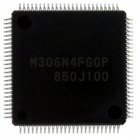
M306N4FGGP#U3 Renesas Electronics America, M306N4FGGP#U3 Datasheet - Page 185

M306N4FGGP#U3
Manufacturer Part Number
M306N4FGGP#U3
Description
IC M16C/6N4 MCU FLASH 100-LQFP
Manufacturer
Renesas Electronics America
Series
M16C™ M16C/6Nr
Specifications of M306N4FGGP#U3
Core Processor
M16C/60
Core Size
16-Bit
Speed
24MHz
Connectivity
CAN, I²C, IEBus, SIO, UART/USART
Peripherals
DMA, WDT
Number Of I /o
85
Program Memory Size
256KB (256K x 8)
Program Memory Type
FLASH
Ram Size
10K x 8
Voltage - Supply (vcc/vdd)
3 V ~ 5.5 V
Data Converters
A/D 26x10b; D/A 2x8b
Oscillator Type
Internal
Operating Temperature
-40°C ~ 85°C
Package / Case
100-LQFP
Package
100LQFP
Family Name
M16C
Maximum Speed
24 MHz
Operating Supply Voltage
3.3|5 V
Data Bus Width
16|32 Bit
Number Of Programmable I/os
87
Interface Type
I2C/UART
On-chip Adc
26-chx10-bit
On-chip Dac
2-chx8-bit
Number Of Timers
11
For Use With
R0K3306NKS001BE - KIT DEV RSK RSK-M16C/6NKR0K3306NKS000BE - KIT DEV RSK RSK-M16C/6NK
Lead Free Status / RoHS Status
Lead free / RoHS Compliant
Eeprom Size
-
Available stocks
Company
Part Number
Manufacturer
Quantity
Price
- Current page: 185 of 414
- Download datasheet (3Mb)
M16C/6N Group (M16C/6N4)
Rev.2.40
REJ09B0009-0240
i = 0 to 2
Table 15.8 P6_4 Pin Functions
-: 0 or 1
NOTE:
Table 15.7 I/O Pin Functions
P6_4
_________
CTS1
_________
RTS1
_________
CTS0
TXDi
(P6_3, P6_7, P7_0)
RXDi
(P6_2, P6_6, P7_1)
CLKi
(P6_1, P6_5, P7_2)
________ ________
CTSi/RTSi
(P6_0, P6_4, P7_3)
Pin Function
1.
Table 15.7 lists the I/O Pins Functions in UART mode. Table 15.8 lists the P6_4 Pin Functions in UART
mode. Note that for a period from when the UARTi operating mode is selected to when transfer starts, the
TXDi pin outputs an “H”.
Figure 15.17 shows the Transmit Operation in UART mode. Figure 15.18 shows the Receive Operation in
UART mode.
Pin Name
In addition to this, set the CRD bit in the U0C0 register to 0 (CTS0/RTS0 enabled) and the CRS
bit in the U0C0 register to 1 (RTS0 selected).
Apr 14, 2006
(1)
Serial data output
Serial data input
I/O port
Transfer clock input
_______
CTS input
________
RTS output
I/O port
CRD bit
page 161 of 376
U1C0 Register
1
0
0
0
Function
CRS bit
_________
0
1
0
-
(Outputs “H” when performing reception only)
Bits PD6_2 and PD6_6 in PD6 register = 0
PD7_1 bit in PD7 register = 0
(Can be used as an input port when performing transmission only)
CKDIR bit in UiMR register = 0
CKDIR bit in UiMR register = 1
Bits PD6_1 and PD6_5 in PD6 register = 0
PD7_2 bit in PD7 register = 0
CRD bit in UiC0 register = 0
CRS bit in UiC0 register = 0
Bits PD6_0 and PD6_4 in PD6 register = 0
PD7_3 bit in PD7 register = 0
CRD bit = 0
CRS bit = 1
CRD bit = 1
RCSP bit CLKMD1 bit
UCON Register
0
0
0
1
Bit set Value
0
0
0
0
Method of Selection
__________ _________
Input: 0, Output: 1
PD6 Register
PD6_4 bit
0
0
-
15. Serial Interface
Related parts for M306N4FGGP#U3
Image
Part Number
Description
Manufacturer
Datasheet
Request
R

Part Number:
Description:
KIT STARTER FOR M16C/29
Manufacturer:
Renesas Electronics America
Datasheet:

Part Number:
Description:
KIT STARTER FOR R8C/2D
Manufacturer:
Renesas Electronics America
Datasheet:

Part Number:
Description:
R0K33062P STARTER KIT
Manufacturer:
Renesas Electronics America
Datasheet:

Part Number:
Description:
KIT STARTER FOR R8C/23 E8A
Manufacturer:
Renesas Electronics America
Datasheet:

Part Number:
Description:
KIT STARTER FOR R8C/25
Manufacturer:
Renesas Electronics America
Datasheet:

Part Number:
Description:
KIT STARTER H8S2456 SHARPE DSPLY
Manufacturer:
Renesas Electronics America
Datasheet:

Part Number:
Description:
KIT STARTER FOR R8C38C
Manufacturer:
Renesas Electronics America
Datasheet:

Part Number:
Description:
KIT STARTER FOR R8C35C
Manufacturer:
Renesas Electronics America
Datasheet:

Part Number:
Description:
KIT STARTER FOR R8CL3AC+LCD APPS
Manufacturer:
Renesas Electronics America
Datasheet:

Part Number:
Description:
KIT STARTER FOR RX610
Manufacturer:
Renesas Electronics America
Datasheet:

Part Number:
Description:
KIT STARTER FOR R32C/118
Manufacturer:
Renesas Electronics America
Datasheet:

Part Number:
Description:
KIT DEV RSK-R8C/26-29
Manufacturer:
Renesas Electronics America
Datasheet:

Part Number:
Description:
KIT STARTER FOR SH7124
Manufacturer:
Renesas Electronics America
Datasheet:

Part Number:
Description:
KIT STARTER FOR H8SX/1622
Manufacturer:
Renesas Electronics America
Datasheet:

Part Number:
Description:
KIT DEV FOR SH7203
Manufacturer:
Renesas Electronics America
Datasheet:


