MC9S12NE64VTU Freescale Semiconductor, MC9S12NE64VTU Datasheet - Page 47
MC9S12NE64VTU
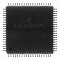
Manufacturer Part Number
MC9S12NE64VTU
Description
IC MCU 25MHZ ETHERNET/PHY 80TQFP
Manufacturer
Freescale Semiconductor
Series
HCS12r
Datasheet
1.MC9S12NE64VTU.pdf
(554 pages)
Specifications of MC9S12NE64VTU
Mfg Application Notes
MC9S12NE64 Integrated Ethernet Controller Implementing an Ethernet Interface with the MC9S12NE64 Web Server Development with MC9S12NE64 and Open TCP
Core Processor
HCS12
Core Size
16-Bit
Speed
25MHz
Connectivity
EBI/EMI, Ethernet, I²C, SCI, SPI
Peripherals
POR, PWM, WDT
Number Of I /o
38
Program Memory Size
64KB (64K x 8)
Program Memory Type
FLASH
Ram Size
8K x 8
Voltage - Supply (vcc/vdd)
2.375 V ~ 3.465 V
Data Converters
A/D 8x10b
Oscillator Type
Internal
Operating Temperature
-40°C ~ 105°C
Package / Case
80-TQFP Exposed Pad, 80-eTQFP, 80-HTQFP, 80-VQFP
Data Bus Width
16 bit
Data Ram Size
8 KB
Interface Type
I2C, SCI, SPI
Maximum Clock Frequency
25 MHz
Number Of Programmable I/os
70
Number Of Timers
16 bit
Operating Supply Voltage
- 0.3 V to + 3 V
Maximum Operating Temperature
+ 105 C
Mounting Style
SMD/SMT
Minimum Operating Temperature
- 65 C
On-chip Adc
10 bit
For Use With
EVB9S12NE64E - BOARD EVAL FOR 9S12NE64DEMO9S12NE64E - DEMO BOARD FOR 9S12NE64
Lead Free Status / RoHS Status
Lead free / RoHS Compliant
Eeprom Size
-
Lead Free Status / Rohs Status
Details
Available stocks
Company
Part Number
Manufacturer
Quantity
Price
Company:

Part Number:
MC9S12NE64VTU
Manufacturer:
FREESCALE
Quantity:
1 831
Company:
Part Number:
MC9S12NE64VTU
Manufacturer:
Freescale Semiconductor
Quantity:
10 000
Company:
Part Number:
MC9S12NE64VTUE
Manufacturer:
Freescale Semiconductor
Quantity:
10 000
Part Number:
MC9S12NE64VTUE
Manufacturer:
FREESCALE
Quantity:
20 000


1.2.3
1.2.3.1
EXTAL and XTAL are the external clock and crystal driver pins. Upon reset, all the device clocks are
derived from the EXTAL input frequency. XTAL is the crystal output.
1.2.3.2
RESET is an active-low bidirectional control signal that acts as an input to initialize the MCU to a known
start-up state. It also acts as an open-drain output to indicate that an internal failure has been detected in
either the clock monitor or COP watchdog circuit. External circuitry connected to the RESET pin must not
include a large capacitance that would interfere with the ability of this signal to rise to a valid logic one
within 32 ECLK cycles after the low drive is released. Upon detection of any reset, an internal circuit
drives the RESET pin low and a clocked reset sequence controls when the MCU can begin normal
processing. The RESET pin includes an internal pull-up device.
1.2.3.3
Dedicated pin used to create the PLL filter. See
description chapter for more detailed information.
1.2.3.4
The BKGD / MODC / TAGHI pin is used as a pseudo-open-drain pin for background debug
communication. It is used as an MCU operating mode select pin during reset. The state of this pin is
latched to the MODC bit at the rising edge of RESET. In MCU expanded modes of operation, while
instruction tagging is on, an input low on this pin during the falling edge of E-clock tags the high half of
the instruction word being read into the instruction queue. This pin always has an internal pull-up.
1.2.3.5
PA[7:0] are general-purpose I/O pins. In MCU expanded modes of operation, these pins are used for the
multiplexed external address and data bus. PA[7:0] pins are not available in the 80-pin package version.
Freescale Semiconductor
Detailed Signal Descriptions
EXTAL, XTAL — Oscillator Pins
RESET — External Reset Pin
XFC — PLL Loop Filter Pin
BKGD / MODC / TAGHI — Background Debug / Tag High / Mode Pin
PA[7:0] / ADDR[15:8] / DATA[15:8] — Port A I/O Pins
Signals shown in bold are not available in the 80-pin package.
If the port pins are not bonded out in the chosen package, the user must
initialize the registers to be inputs with enabled pull resistance to avoid
excess current consumption. This applies to the following pins:
(80-Pin TQFP-EP): Port A[7:0], Port B[7:0], Port E[7,6,5,3,2], Port K[7:0];
Port G[7]; Port L[6:5]
MC9S12NE64 Data Sheet, Rev 1.0
A.12.3.1, “XFC Component
NOTE
NOTE
Selection,” and the CRG block
Signal Description
47
Related parts for MC9S12NE64VTU
Image
Part Number
Description
Manufacturer
Datasheet
Request
R

Part Number:
Description:
Manufacturer:
Freescale Semiconductor, Inc
Datasheet:
Part Number:
Description:
Manufacturer:
Freescale Semiconductor, Inc
Datasheet:
Part Number:
Description:
Manufacturer:
Freescale Semiconductor, Inc
Datasheet:
Part Number:
Description:
Manufacturer:
Freescale Semiconductor, Inc
Datasheet:
Part Number:
Description:
Manufacturer:
Freescale Semiconductor, Inc
Datasheet:
Part Number:
Description:
Manufacturer:
Freescale Semiconductor, Inc
Datasheet:
Part Number:
Description:
Manufacturer:
Freescale Semiconductor, Inc
Datasheet:
Part Number:
Description:
Manufacturer:
Freescale Semiconductor, Inc
Datasheet:
Part Number:
Description:
Manufacturer:
Freescale Semiconductor, Inc
Datasheet:
Part Number:
Description:
Manufacturer:
Freescale Semiconductor, Inc
Datasheet:
Part Number:
Description:
Manufacturer:
Freescale Semiconductor, Inc
Datasheet:
Part Number:
Description:
Manufacturer:
Freescale Semiconductor, Inc
Datasheet:
Part Number:
Description:
Manufacturer:
Freescale Semiconductor, Inc
Datasheet:
Part Number:
Description:
Manufacturer:
Freescale Semiconductor, Inc
Datasheet:
Part Number:
Description:
Manufacturer:
Freescale Semiconductor, Inc
Datasheet: