MC9S12NE64VTU Freescale Semiconductor, MC9S12NE64VTU Datasheet - Page 120
MC9S12NE64VTU
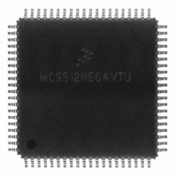
Manufacturer Part Number
MC9S12NE64VTU
Description
IC MCU 25MHZ ETHERNET/PHY 80TQFP
Manufacturer
Freescale Semiconductor
Series
HCS12r
Datasheet
1.MC9S12NE64VTU.pdf
(554 pages)
Specifications of MC9S12NE64VTU
Mfg Application Notes
MC9S12NE64 Integrated Ethernet Controller Implementing an Ethernet Interface with the MC9S12NE64 Web Server Development with MC9S12NE64 and Open TCP
Core Processor
HCS12
Core Size
16-Bit
Speed
25MHz
Connectivity
EBI/EMI, Ethernet, I²C, SCI, SPI
Peripherals
POR, PWM, WDT
Number Of I /o
38
Program Memory Size
64KB (64K x 8)
Program Memory Type
FLASH
Ram Size
8K x 8
Voltage - Supply (vcc/vdd)
2.375 V ~ 3.465 V
Data Converters
A/D 8x10b
Oscillator Type
Internal
Operating Temperature
-40°C ~ 105°C
Package / Case
80-TQFP Exposed Pad, 80-eTQFP, 80-HTQFP, 80-VQFP
Data Bus Width
16 bit
Data Ram Size
8 KB
Interface Type
I2C, SCI, SPI
Maximum Clock Frequency
25 MHz
Number Of Programmable I/os
70
Number Of Timers
16 bit
Operating Supply Voltage
- 0.3 V to + 3 V
Maximum Operating Temperature
+ 105 C
Mounting Style
SMD/SMT
Minimum Operating Temperature
- 65 C
On-chip Adc
10 bit
For Use With
EVB9S12NE64E - BOARD EVAL FOR 9S12NE64DEMO9S12NE64E - DEMO BOARD FOR 9S12NE64
Lead Free Status / RoHS Status
Lead free / RoHS Compliant
Eeprom Size
-
Lead Free Status / Rohs Status
Details
Available stocks
Company
Part Number
Manufacturer
Quantity
Price
Company:

Part Number:
MC9S12NE64VTU
Manufacturer:
FREESCALE
Quantity:
1 831
Company:
Part Number:
MC9S12NE64VTU
Manufacturer:
Freescale Semiconductor
Quantity:
10 000
Company:
Part Number:
MC9S12NE64VTUE
Manufacturer:
Freescale Semiconductor
Quantity:
10 000
Part Number:
MC9S12NE64VTUE
Manufacturer:
FREESCALE
Quantity:
20 000


Chapter 3 Port Integration Module (PIM9NE64V1)
3.3.2.3.2
Read:Anytime.
Write:Never, writes to this register have no effect.
This register always reads back the status of the associated pins. This also can be used to detect overload
or short circuit conditions on output pins.
3.3.2.3.3
Read:Anytime.
Write:Anytime.
This register configures each port G pin as either input or output.
DDRG[7:0] — Data Direction Port G
If the EMAC MII external interface is enabled, the pins G[6:0] are forced to be inputs and DDRG has no
effect on the them. Please refer to the EMAC block description chapter for details.
The DDRG bits revert to controlling the I/O direction of a pin when the EMAC MII external interface is
disabled.
Due to internal synchronization circuits, it can take up to 2 bus cycles until the correct value is read on PTG
or PTIG registers, when changing the DDRG register.
120
1 = Associated pin is configured as output.
0 = Associated pin is configured as input.
Module Base + $11
Module Base + $12
Reset:
Reset:
Read:
Read:
Write:
Write:
Input Register (PTIG)
Data Direction Register (DDRG)
DDRG7
PTIG7
Bit 7
Bit 7
—
0
= Reserved or unimplemented
DDRG6
Figure 3-17. Port G Data Direction Register (DDRG)
PTIG6
—
6
6
0
Figure 3-16. Port G Input Register (PTIG)
MC9S12NE64 Data Sheet, Rev. 1.1
DDRG5
PTIG5
—
5
5
0
DDRG4
PTIG4
—
4
4
0
DDRG3
PTIG3
—
3
3
0
DDRG2
PTIG2
—
2
2
0
DDRG1
PTIG1
—
1
1
0
Freescale Semiconductor
DDRG0
PTIG0
Bit 0
Bit 0
—
0
Related parts for MC9S12NE64VTU
Image
Part Number
Description
Manufacturer
Datasheet
Request
R

Part Number:
Description:
Manufacturer:
Freescale Semiconductor, Inc
Datasheet:
Part Number:
Description:
Manufacturer:
Freescale Semiconductor, Inc
Datasheet:
Part Number:
Description:
Manufacturer:
Freescale Semiconductor, Inc
Datasheet:
Part Number:
Description:
Manufacturer:
Freescale Semiconductor, Inc
Datasheet:
Part Number:
Description:
Manufacturer:
Freescale Semiconductor, Inc
Datasheet:
Part Number:
Description:
Manufacturer:
Freescale Semiconductor, Inc
Datasheet:
Part Number:
Description:
Manufacturer:
Freescale Semiconductor, Inc
Datasheet:
Part Number:
Description:
Manufacturer:
Freescale Semiconductor, Inc
Datasheet:
Part Number:
Description:
Manufacturer:
Freescale Semiconductor, Inc
Datasheet:
Part Number:
Description:
Manufacturer:
Freescale Semiconductor, Inc
Datasheet:
Part Number:
Description:
Manufacturer:
Freescale Semiconductor, Inc
Datasheet:
Part Number:
Description:
Manufacturer:
Freescale Semiconductor, Inc
Datasheet:
Part Number:
Description:
Manufacturer:
Freescale Semiconductor, Inc
Datasheet:
Part Number:
Description:
Manufacturer:
Freescale Semiconductor, Inc
Datasheet:
Part Number:
Description:
Manufacturer:
Freescale Semiconductor, Inc
Datasheet: