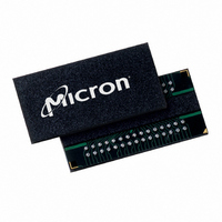
MT41J256M4HX-15E:D TR Micron Technology Inc, MT41J256M4HX-15E:D TR Datasheet - Page 24

MT41J256M4HX-15E:D TR
Manufacturer Part Number
MT41J256M4HX-15E:D TR
Description
IC DDR3 SDRAM 1GBIT 78FBGA
Manufacturer
Micron Technology Inc
Type
DDR3 SDRAMr
Specifications of MT41J256M4HX-15E:D TR
Format - Memory
RAM
Memory Type
DDR3 SDRAM
Memory Size
1G (256M x 4)
Speed
667MHz
Interface
Parallel
Voltage - Supply
1.425 V ~ 1.575 V
Operating Temperature
0°C ~ 95°C
Package / Case
78-FBGA
Organization
256Mx4
Density
1Gb
Address Bus
17b
Maximum Clock Rate
1.333GHz
Operating Supply Voltage (typ)
1.5V
Package Type
FBGA
Operating Temp Range
0C to 95C
Operating Supply Voltage (max)
1.575V
Operating Supply Voltage (min)
1.425V
Supply Current
220mA
Pin Count
78
Mounting
Surface Mount
Operating Temperature Classification
Commercial
Lead Free Status / RoHS Status
Lead free / RoHS Compliant
- Current page: 24 of 208
- Download datasheet (13Mb)
Table 5: 96-Ball FBGA – x16 Ball Descriptions (Continued)
PDF: 09005aef826aa906
1Gb_DDR3_SDRAM.pdf – Rev. J 05/10 EN
DQ13, DQ14, DQ15
DQ8, DQ9, DQ10,
DQ0, DQ1, DQ2,
DQ3, DQ4, DQ5,
UDQS, UDQS#
DQ11, DQ12,
LDQS, LDQS#
DQ6, DQ7
Symbol
V
V
UDM
V
V
V
REFDQ
REFCA
V
ZQ
NC
DDQ
SSQ
DD
SS
Reference
Supply
Supply
Supply
Supply
Supply
Supply
Type
Input
I/O
I/O
I/O
I/O
–
Description
Input data mask: UDM is an upper-byte, input mask signal for write data. Upper-
byte input data is masked when UDM is sampled HIGH along with that input data
during a WRITE access. Although the UDM ball is input-only, the UDM loading is
designed to match that of the DQ and DQS balls. UDM is referenced to V
Data input/output: Lower byte of bidirectional data bus for the x16 configuration.
DQ[7:0] are referenced to V
Data input/output: Upper byte of bidirectional data bus for the x16 configuration.
DQ[15:8] are referenced to V
Lower byte data strobe: Output with read data. Edge-aligned with read data.
Input with write data. Center-aligned to write data.
Upper byte data strobe: Output with read data. Edge-aligned with read data.
Input with write data. DQS is center-aligned to write data.
Power supply: 1.5V ±0.075V.
DQ power supply: 1.5V ±0.075V. Isolated on the device for improved noise immunity.
Reference voltage for control, command, and address: V
maintained at all times (including self refresh) for proper device operation.
Reference voltage for data: V
refresh) for proper device operation.
Ground.
DQ ground: Isolated on the device for improved noise immunity.
External reference ball for output drive calibration: This ball is tied to an
external 240Ω resistor (RZQ), which is tied to V
No connect: These balls should be left unconnected (the ball has no connection to
the DRAM or to other balls).
24
REFDQ
REFDQ
REFDQ
.
.
Micron Technology, Inc. reserves the right to change products or specifications without notice.
Ball Assignments and Descriptions
must be maintained at all times (excluding self
1Gb: x4, x8, x16 DDR3 SDRAM
SSQ
.
© 2006 Micron Technology, Inc. All rights reserved.
REFCA
must be
REFDQ
.
Related parts for MT41J256M4HX-15E:D TR
Image
Part Number
Description
Manufacturer
Datasheet
Request
R

Part Number:
Description:
Manufacturer:
Micron Technology Inc
Datasheet:

Part Number:
Description:
Manufacturer:
Micron Technology Inc
Datasheet:

Part Number:
Description:
IC SDRAM 64MBIT 133MHZ 54TSOP
Manufacturer:
Micron Technology Inc
Datasheet:

Part Number:
Description:
IC SDRAM 64MBIT 5.5NS 86TSOP
Manufacturer:
Micron Technology Inc
Datasheet:

Part Number:
Description:
IC SDRAM 64MBIT 200MHZ 86TSOP
Manufacturer:
Micron Technology Inc
Datasheet:

Part Number:
Description:
IC SDRAM 64MBIT 133MHZ 54TSOP
Manufacturer:
Micron Technology Inc
Datasheet:

Part Number:
Description:
IC SDRAM 128MBIT 133MHZ 54TSOP
Manufacturer:
Micron Technology Inc
Datasheet:

Part Number:
Description:
IC SDRAM 256MBIT 133MHZ 90VFBGA
Manufacturer:
Micron Technology Inc
Datasheet:

Part Number:
Description:
IC SDRAM 128MBIT 133MHZ 54TSOP
Manufacturer:
Micron Technology Inc
Datasheet:

Part Number:
Description:
IC SDRAM 256MBIT 133MHZ 54TSOP
Manufacturer:
Micron Technology Inc
Datasheet:

Part Number:
Description:
IC DDR SDRAM 512MBIT 6NS 66TSOP
Manufacturer:
Micron Technology Inc
Datasheet:

Part Number:
Description:
IC SDRAM 128MBIT 167MHZ 86TSOP
Manufacturer:
Micron Technology Inc
Datasheet:

Part Number:
Description:
IC SDRAM 128MBIT 143MHZ 86TSOP
Manufacturer:
Micron Technology Inc
Datasheet:

Part Number:
Description:
SDRAM 256M-BIT 1.8V 54-PIN VFBGA
Manufacturer:
Micron Technology Inc
Datasheet:

Part Number:
Description:
IC SDRAM 128MBIT 143MHZ 86TSOP
Manufacturer:
Micron Technology Inc
Datasheet:


