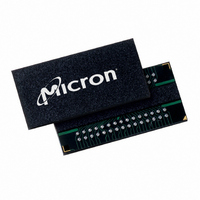
MT41J256M4HX-15E:D TR Micron Technology Inc, MT41J256M4HX-15E:D TR Datasheet - Page 164

MT41J256M4HX-15E:D TR
Manufacturer Part Number
MT41J256M4HX-15E:D TR
Description
IC DDR3 SDRAM 1GBIT 78FBGA
Manufacturer
Micron Technology Inc
Type
DDR3 SDRAMr
Specifications of MT41J256M4HX-15E:D TR
Format - Memory
RAM
Memory Type
DDR3 SDRAM
Memory Size
1G (256M x 4)
Speed
667MHz
Interface
Parallel
Voltage - Supply
1.425 V ~ 1.575 V
Operating Temperature
0°C ~ 95°C
Package / Case
78-FBGA
Organization
256Mx4
Density
1Gb
Address Bus
17b
Maximum Clock Rate
1.333GHz
Operating Supply Voltage (typ)
1.5V
Package Type
FBGA
Operating Temp Range
0C to 95C
Operating Supply Voltage (max)
1.575V
Operating Supply Voltage (min)
1.425V
Supply Current
220mA
Pin Count
78
Mounting
Surface Mount
Operating Temperature Classification
Commercial
Lead Free Status / RoHS Status
Lead free / RoHS Compliant
- Current page: 164 of 208
- Download datasheet (13Mb)
WRITE Operation
PDF: 09005aef826aa906
1Gb_DDR3_SDRAM.pdf – Rev. J 05/10 EN
WRITE bursts are initiated with a WRITE command. The starting column and bank ad-
dresses are provided with the WRITE command, and auto precharge is either enabled
or disabled for that access. If auto precharge is selected, the row being accessed will be
precharged at the end of the WRITE burst. If auto precharge is not selected, the row will
remain open for subsequent accesses. After a WRITE command has been issued, the
WRITE burst may not be interrupted. For the generic WRITE commands used in Fig-
ure 85 (page 166) through Figure 93 (page 171), auto precharge is disabled.
During WRITE bursts, the first valid data-in element is registered on a rising edge of
DQS following the WRITE latency (WL) clocks later and subsequent data elements will
be registered on successive edges of DQS. WRITE latency (WL) is defined as the sum of
POSTED CAS ADDITIVE latency (AL) and CAS WRITE latency (CWL): WL = AL + CWL.
The values of AL and CWL are programmed in the MR0 and MR2 registers, respectively.
Prior to the first valid DQS edge, a full cycle is needed (including a dummy crossover of
DQS, DQS#) and specified as the WRITE preamble shown in Figure 85 (page 166). The
half cycle on DQS following the last data-in element is known as the WRITE postamble.
The time between the WRITE command and the first valid edge of DQS is WL clocks
±
where
(MAX) cases.
Data may be masked from completing a WRITE using data mask. The mask occurs on
the DM ball aligned to the write data. If DM is LOW, the write completes normally. If
DM is HIGH, that bit of data is masked.
Upon completion of a burst, assuming no other commands have been initiated, the DQ
will remain High-Z, and any additional input data will be ignored.
Data for any WRITE burst may be concatenated with a subsequent WRITE command to
provide a continuous flow of input data. The new WRITE command can be
following the previous WRITE command. The first data element from the new burst is
applied after the last element of a completed burst. Figure 86 (page 167) and Figure 87
(page 167) on Figure 87 (page 167) show concatenated bursts. An example of noncon-
secutive WRITEs is shown in Figure 88 (page 168).
Data for any WRITE burst may be followed by a subsequent READ command after
has been met (see Figure 89 (page 168) and Figure 90 (page 169) on Figure 90
(page 169) and Figure 91 (page 170)).
Data for any WRITE burst may be followed by a subsequent PRECHARGE command
providing
(page 171).
Both
(fixed BC4, BL8 versus OTF).
t
DQSS. Figure 86 (page 167) through Figure 93 (page 171) show the nominal case
t
WTR and
t
DQSS = 0ns; however, Figure 85 (page 166) includes
t
WR has been met, as shown in Figure 92 (page 171) and Figure 93
t
WR starting time may vary depending on the mode register settings
164
Micron Technology, Inc. reserves the right to change products or specifications without notice.
1Gb: x4, x8, x16 DDR3 SDRAM
t
DQSS (MIN) and
© 2006 Micron Technology, Inc. All rights reserved.
WRITE Operation
t
CCD clocks
t
DQSS
t
WTR
Related parts for MT41J256M4HX-15E:D TR
Image
Part Number
Description
Manufacturer
Datasheet
Request
R

Part Number:
Description:
Manufacturer:
Micron Technology Inc
Datasheet:

Part Number:
Description:
Manufacturer:
Micron Technology Inc
Datasheet:

Part Number:
Description:
IC SDRAM 64MBIT 133MHZ 54TSOP
Manufacturer:
Micron Technology Inc
Datasheet:

Part Number:
Description:
IC SDRAM 64MBIT 5.5NS 86TSOP
Manufacturer:
Micron Technology Inc
Datasheet:

Part Number:
Description:
IC SDRAM 64MBIT 200MHZ 86TSOP
Manufacturer:
Micron Technology Inc
Datasheet:

Part Number:
Description:
IC SDRAM 64MBIT 133MHZ 54TSOP
Manufacturer:
Micron Technology Inc
Datasheet:

Part Number:
Description:
IC SDRAM 128MBIT 133MHZ 54TSOP
Manufacturer:
Micron Technology Inc
Datasheet:

Part Number:
Description:
IC SDRAM 256MBIT 133MHZ 90VFBGA
Manufacturer:
Micron Technology Inc
Datasheet:

Part Number:
Description:
IC SDRAM 128MBIT 133MHZ 54TSOP
Manufacturer:
Micron Technology Inc
Datasheet:

Part Number:
Description:
IC SDRAM 256MBIT 133MHZ 54TSOP
Manufacturer:
Micron Technology Inc
Datasheet:

Part Number:
Description:
IC DDR SDRAM 512MBIT 6NS 66TSOP
Manufacturer:
Micron Technology Inc
Datasheet:

Part Number:
Description:
IC SDRAM 128MBIT 167MHZ 86TSOP
Manufacturer:
Micron Technology Inc
Datasheet:

Part Number:
Description:
IC SDRAM 128MBIT 143MHZ 86TSOP
Manufacturer:
Micron Technology Inc
Datasheet:

Part Number:
Description:
SDRAM 256M-BIT 1.8V 54-PIN VFBGA
Manufacturer:
Micron Technology Inc
Datasheet:

Part Number:
Description:
IC SDRAM 128MBIT 143MHZ 86TSOP
Manufacturer:
Micron Technology Inc
Datasheet:


