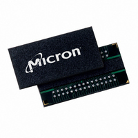
MT41J256M4HX-15E:D TR Micron Technology Inc, MT41J256M4HX-15E:D TR Datasheet - Page 103

MT41J256M4HX-15E:D TR
Manufacturer Part Number
MT41J256M4HX-15E:D TR
Description
IC DDR3 SDRAM 1GBIT 78FBGA
Manufacturer
Micron Technology Inc
Type
DDR3 SDRAMr
Specifications of MT41J256M4HX-15E:D TR
Format - Memory
RAM
Memory Type
DDR3 SDRAM
Memory Size
1G (256M x 4)
Speed
667MHz
Interface
Parallel
Voltage - Supply
1.425 V ~ 1.575 V
Operating Temperature
0°C ~ 95°C
Package / Case
78-FBGA
Organization
256Mx4
Density
1Gb
Address Bus
17b
Maximum Clock Rate
1.333GHz
Operating Supply Voltage (typ)
1.5V
Package Type
FBGA
Operating Temp Range
0C to 95C
Operating Supply Voltage (max)
1.575V
Operating Supply Voltage (min)
1.425V
Supply Current
220mA
Pin Count
78
Mounting
Surface Mount
Operating Temperature Classification
Commercial
Lead Free Status / RoHS Status
Lead free / RoHS Compliant
- Current page: 103 of 208
- Download datasheet (13Mb)
Data Setup, Hold, and Derating
Table 62: Data Setup and Hold Values at 1 V/ns (DQS, DQS# at 2 V/ns) – AC/DC-Based
PDF: 09005aef826aa906
1Gb_DDR3_SDRAM.pdf – Rev. J 05/10 EN
t
t
t
DS (base) AC175
DS (base) AC150
DS (base) AC135
t
DH (base)
Symbol
DC100
DDR3-800
125
150
75
–
The total
sheet
ble 54 (page 76)) to the Δ
respectively. Example:
the input signal has to remain above/below V
ble 66 (page 105)).
Although the total setup time for slow slew rates might be negative (for example, a valid
input signal will not have reached V
tion), a valid input signal is still required to complete the transition and to reach V
V
derating values may obtained by linear interpolation.
Setup (
last crossing of V
rate for a falling signal is defined as the slew rate between the last crossing of V
and the first crossing of V
slew rate line between the shaded “V
for derating value (see Figure 38 (page 106)). If the actual signal is later than the nomi-
nal slew rate line anywhere between the shaded “V
of a tangent line to the actual signal from the AC level to the DC level is used for derat-
ing value (see Figure 40 (page 108)).
Hold (
last crossing of V
rate for a falling signal is defined as the slew rate between the last crossing of V
and the first crossing of V
slew rate line between the shaded “DC-to-V
for derating value (see Figure 39 (page 107)). If the actual signal is earlier than the nom-
inal slew rate line anywhere between the shaded “DC-to-V
of a tangent line to the actual signal from the “DC-to-V
ing value (see Figure 41 (page 109)).
IL(AC)
DDR3-1066 DDR3-1333
t
. For slew rates which fall between the values listed in Table 64 (page 104), the
t
DS (base) and
DH) nominal slew rate for a rising signal is defined as the slew rate between the
t
DS) nominal slew rate for a rising signal is defined as the slew rate between the
100
25
75
–
t
DS (setup time) and
REF(DC)
IL(DC)max
t
30
65
DH (base) values (see Table 62 (page 103); values come from Ta-
–
–
t
DS (total setup time) =
and the first crossing of V
t
IL(AC)max
REF(DC)
DS and Δ
and the first crossing of V
103
DDR3-1600
t
DH (hold time) required is calculated by adding the data
. If the actual signal is always later than the nominal
. If the actual signal is always earlier than the nominal
10
45
t
–
–
DH derating values (see Table 63 (page 104)),
IH(AC)
REF(DC)
Micron Technology, Inc. reserves the right to change products or specifications without notice.
/V
IL(AC)
-to-AC region,” use the nominal slew rate
REF(DC)
DDR3-1866
Data Setup, Hold, and Derating
IH(AC)
t
1Gb: x4, x8, x16 DDR3 SDRAM
DS (base) + Δ
) at the time of the rising clock transi-
20
IH(AC)min
0
–
–
/V
REF(DC)
REF(DC)
region,” use the nominal slew rate
IL(AC)
REF(DC)
-to-AC region,” the slew rate
. Setup (
. Hold (
REF(DC)
for some time
Units
t
DS. For a valid transition,
© 2006 Micron Technology, Inc. All rights reserved.
region” is used for derat-
ps
ps
ps
ps
t
DH) nominal slew
region,” the slew rate
t
DS) nominal slew
V
V
V
V
t
Reference
VAC (see Ta-
IH(AC)
IH(AC)
IH(AC)
IH(DC)
/V
/V
/V
/V
REF(DC)
IH(DC)min
IL(AC)
IL(AC)
IL(AC)
IL(DC)
IH
/
Related parts for MT41J256M4HX-15E:D TR
Image
Part Number
Description
Manufacturer
Datasheet
Request
R

Part Number:
Description:
Manufacturer:
Micron Technology Inc
Datasheet:

Part Number:
Description:
Manufacturer:
Micron Technology Inc
Datasheet:

Part Number:
Description:
IC SDRAM 64MBIT 133MHZ 54TSOP
Manufacturer:
Micron Technology Inc
Datasheet:

Part Number:
Description:
IC SDRAM 64MBIT 5.5NS 86TSOP
Manufacturer:
Micron Technology Inc
Datasheet:

Part Number:
Description:
IC SDRAM 64MBIT 200MHZ 86TSOP
Manufacturer:
Micron Technology Inc
Datasheet:

Part Number:
Description:
IC SDRAM 64MBIT 133MHZ 54TSOP
Manufacturer:
Micron Technology Inc
Datasheet:

Part Number:
Description:
IC SDRAM 128MBIT 133MHZ 54TSOP
Manufacturer:
Micron Technology Inc
Datasheet:

Part Number:
Description:
IC SDRAM 256MBIT 133MHZ 90VFBGA
Manufacturer:
Micron Technology Inc
Datasheet:

Part Number:
Description:
IC SDRAM 128MBIT 133MHZ 54TSOP
Manufacturer:
Micron Technology Inc
Datasheet:

Part Number:
Description:
IC SDRAM 256MBIT 133MHZ 54TSOP
Manufacturer:
Micron Technology Inc
Datasheet:

Part Number:
Description:
IC DDR SDRAM 512MBIT 6NS 66TSOP
Manufacturer:
Micron Technology Inc
Datasheet:

Part Number:
Description:
IC SDRAM 128MBIT 167MHZ 86TSOP
Manufacturer:
Micron Technology Inc
Datasheet:

Part Number:
Description:
IC SDRAM 128MBIT 143MHZ 86TSOP
Manufacturer:
Micron Technology Inc
Datasheet:

Part Number:
Description:
SDRAM 256M-BIT 1.8V 54-PIN VFBGA
Manufacturer:
Micron Technology Inc
Datasheet:

Part Number:
Description:
IC SDRAM 128MBIT 143MHZ 86TSOP
Manufacturer:
Micron Technology Inc
Datasheet:


