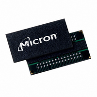
MT41J256M4HX-15E:D TR Micron Technology Inc, MT41J256M4HX-15E:D TR Datasheet - Page 142

MT41J256M4HX-15E:D TR
Manufacturer Part Number
MT41J256M4HX-15E:D TR
Description
IC DDR3 SDRAM 1GBIT 78FBGA
Manufacturer
Micron Technology Inc
Type
DDR3 SDRAMr
Specifications of MT41J256M4HX-15E:D TR
Format - Memory
RAM
Memory Type
DDR3 SDRAM
Memory Size
1G (256M x 4)
Speed
667MHz
Interface
Parallel
Voltage - Supply
1.425 V ~ 1.575 V
Operating Temperature
0°C ~ 95°C
Package / Case
78-FBGA
Organization
256Mx4
Density
1Gb
Address Bus
17b
Maximum Clock Rate
1.333GHz
Operating Supply Voltage (typ)
1.5V
Package Type
FBGA
Operating Temp Range
0C to 95C
Operating Supply Voltage (max)
1.575V
Operating Supply Voltage (min)
1.425V
Supply Current
220mA
Pin Count
78
Mounting
Surface Mount
Operating Temperature Classification
Commercial
Lead Free Status / RoHS Status
Lead free / RoHS Compliant
- Current page: 142 of 208
- Download datasheet (13Mb)
Figure 60: Multipurpose Register (MPR) Block Diagram
Table 74: MPR Functional Description of MR3 Bits
MPR Functional Description
PDF: 09005aef826aa906
1Gb_DDR3_SDRAM.pdf – Rev. J 05/10 EN
MR3[2]
MPR
0
1
(see Table 75 (page 143))
MPR READ Function
“Don’t Care”
Notes:
MR3[1:0]
A[1:0]
but outputs MPR data as defined by MR3[0, 1]. If MR3[0, 1] is equal to 00, then a prede-
fined read pattern for system calibration is selected.
To enable the MPR, the MRS command is issued to MR3, and MR3[2] = 1. Prior to issu-
ing the MRS command, all banks must be in the idle state (all banks are precharged,
and
are redirected to the multipurpose register. The resulting operation when either a READ
or a RDAP command is issued, is defined by MR3[1:0] when the MPR is enabled (see
Table 75 (page 143)). When the MPR is enabled, only READ or RDAP commands are
allowed until a subsequent MRS command is issued with the MPR disabled (MR3[2] =
0). Power-down mode, self refresh, and any other nonREAD/RDAP commands are not
allowed during MPR enable mode. The RESET function is supported during MPR ena-
ble mode.
The MPR JEDEC definition enables either a prime DQ (DQ0 on a x4 and a x8; on a x16,
DQ0 = lower byte and DQ8 = upper byte) to output the MPR data with the remaining
Memory core
1. A predefined data pattern can be read out of the MPR with an external READ command.
2. MR3[2] defines whether the data flow comes from the memory core or the MPR. When
t
RP is met). When the MPR is enabled, any subsequent READ or RDAP commands
the data flow is defined, the MPR contents can be read out continuously with a regular
READ or RDAP command.
DQ, DM, DQS, DQS#
MR3[2] = 1 (MPR on)
Enable MPR mode, subsequent READ/RDAP commands defined by bits 1 and 2
MR3[2] = 0 (MPR off)
All subsequent READs come from the DRAM memory array
All subsequent WRITEs go to the DRAM memory array
142
predefined data for READs
Normal operation, no MPR transaction
Multipurpose register
Micron Technology, Inc. reserves the right to change products or specifications without notice.
Function
1Gb: x4, x8, x16 DDR3 SDRAM
Mode Register 3 (MR3)
© 2006 Micron Technology, Inc. All rights reserved.
Related parts for MT41J256M4HX-15E:D TR
Image
Part Number
Description
Manufacturer
Datasheet
Request
R

Part Number:
Description:
Manufacturer:
Micron Technology Inc
Datasheet:

Part Number:
Description:
Manufacturer:
Micron Technology Inc
Datasheet:

Part Number:
Description:
IC SDRAM 64MBIT 133MHZ 54TSOP
Manufacturer:
Micron Technology Inc
Datasheet:

Part Number:
Description:
IC SDRAM 64MBIT 5.5NS 86TSOP
Manufacturer:
Micron Technology Inc
Datasheet:

Part Number:
Description:
IC SDRAM 64MBIT 200MHZ 86TSOP
Manufacturer:
Micron Technology Inc
Datasheet:

Part Number:
Description:
IC SDRAM 64MBIT 133MHZ 54TSOP
Manufacturer:
Micron Technology Inc
Datasheet:

Part Number:
Description:
IC SDRAM 128MBIT 133MHZ 54TSOP
Manufacturer:
Micron Technology Inc
Datasheet:

Part Number:
Description:
IC SDRAM 256MBIT 133MHZ 90VFBGA
Manufacturer:
Micron Technology Inc
Datasheet:

Part Number:
Description:
IC SDRAM 128MBIT 133MHZ 54TSOP
Manufacturer:
Micron Technology Inc
Datasheet:

Part Number:
Description:
IC SDRAM 256MBIT 133MHZ 54TSOP
Manufacturer:
Micron Technology Inc
Datasheet:

Part Number:
Description:
IC DDR SDRAM 512MBIT 6NS 66TSOP
Manufacturer:
Micron Technology Inc
Datasheet:

Part Number:
Description:
IC SDRAM 128MBIT 167MHZ 86TSOP
Manufacturer:
Micron Technology Inc
Datasheet:

Part Number:
Description:
IC SDRAM 128MBIT 143MHZ 86TSOP
Manufacturer:
Micron Technology Inc
Datasheet:

Part Number:
Description:
SDRAM 256M-BIT 1.8V 54-PIN VFBGA
Manufacturer:
Micron Technology Inc
Datasheet:

Part Number:
Description:
IC SDRAM 128MBIT 143MHZ 86TSOP
Manufacturer:
Micron Technology Inc
Datasheet:


