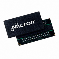
MT41J256M4HX-15E:D TR Micron Technology Inc, MT41J256M4HX-15E:D TR Datasheet - Page 15

MT41J256M4HX-15E:D TR
Manufacturer Part Number
MT41J256M4HX-15E:D TR
Description
IC DDR3 SDRAM 1GBIT 78FBGA
Manufacturer
Micron Technology Inc
Type
DDR3 SDRAMr
Specifications of MT41J256M4HX-15E:D TR
Format - Memory
RAM
Memory Type
DDR3 SDRAM
Memory Size
1G (256M x 4)
Speed
667MHz
Interface
Parallel
Voltage - Supply
1.425 V ~ 1.575 V
Operating Temperature
0°C ~ 95°C
Package / Case
78-FBGA
Organization
256Mx4
Density
1Gb
Address Bus
17b
Maximum Clock Rate
1.333GHz
Operating Supply Voltage (typ)
1.5V
Package Type
FBGA
Operating Temp Range
0C to 95C
Operating Supply Voltage (max)
1.575V
Operating Supply Voltage (min)
1.425V
Supply Current
220mA
Pin Count
78
Mounting
Surface Mount
Operating Temperature Classification
Commercial
Lead Free Status / RoHS Status
Lead free / RoHS Compliant
- Current page: 15 of 208
- Download datasheet (13Mb)
Figure 4: 128 Meg x 8 Functional Block Diagram
RZQ
Figure 5: 64 Meg x 16 Functional Block Diagram
RZQ
PDF: 09005aef826aa906
1Gb_DDR3_SDRAM.pdf – Rev. J 05/10 EN
V
V
SSQ
SSQ
A[13:0]
BA[2:0]
A[12:0]
BA[2:0]
ZQ
CK, CK#
CK, CK#
ZQ
RESET#
RESET#
RAS#
CAS#
RAS#
CAS#
ODT
WE#
ODT
WE#
CKE
A12
CKE
A12
CS#
CS#
17
16
Address
Address
register
register
Mode registers
Mode registers
Control
Control
logic
logic
16
16
14
13
Refresh
counter
Refresh
counter
ZQCL, ZQCS
ZQCL, ZQCS
10
10
3
3
BC4 (burst chop)
OTF
BC4 (burst chop)
OTF
13
14
address
3
address
3
Row-
Row-
MUX
MUX
Column-
Column-
counter/
counter/
address
address
control
control
14
13
Bank
latch
Bank
logic
latch
logic
ZQ CAL
ZQ CAL
address
decoder
decoder
Bank 0
address
Bank 0
row-
latch
and
latch
row-
and
Bank 1
Bank 1
Bank 2
Bank 2
7
7
3
3
Bank 3
Bank 3
Bank 4
Bank 4
16,384
8,192
Bank 5
Bank 5
Bank 6
Bank 6
Columns 0, 1, and 2
Columns 0, 1, and 2
Bank 7
Bank 7
To ODT/output drivers
(16,384 x 128 x 64)
To ODT/output drivers
(8192 x 128 x 128)
Sense amplifiers
Sense amplifiers
DM mask logic
DM mask logic
I/O gating
I/O gating
decoder
Column
decoder
memory
Column
memory
Bank 0
16,384
Bank 0
x128)
array
(128
array
8,192
(128
x64)
Bank 1
Bank 1
Bank 2
Bank 2
Bank 3
Bank 3
Bank 4
Bank 4
Bank 5
Bank 5
15
Bank 6
Bank 6
Bank 7
Bank 7
128
64
BC4
OTF
BC4
OTF
Micron Technology, Inc. reserves the right to change products or specifications without notice.
128
64
128
64
Columns 0, 1, and 2
Column 0, 1, and 2
interface
interface
CK, CK#
READ
CK, CK#
MUX
READ
Data
FIFO
data
MUX
and
FIFO
data
Data
and
1Gb: x4, x8, x16 DDR3 SDRAM
Data
Data
16
8
lower nibble for BC4)
16
8
lower nibble for BC4)
Functional Block Diagrams
(select upper or
(select upper or
Column 2
Column 2
drivers
WRITE
drivers
input
WRITE
logic
input
and
logic
and
control
control
ODT
ODT
CK, CK#
CK, CK#
drivers
READ
drivers
READ
DLL
BC4
DLL
BC4
© 2006 Micron Technology, Inc. All rights reserved.
DQ[15:0]
LDQS, LDQS#, UDQS, UDQS#
DQ[7:0]
DQS, DQS#
sw1
sw1
sw1
sw1
sw1
sw1
R
R
R
R
R
V
V
R
V
V
V
TT,nom
TT,nom
TT,nom
V
TT,nom
TT,nom
DDQ
TT,nom
DDQ
DDQ
DDQ
DDQ
DDQ
/2
/2
/2
/2
/2
/2
DQ8
R
R
R
R
R
R
sw2
sw2
sw2
sw2
TT(WR)
sw2
TT(WR)
sw2
TT(WR)
TT(WR)
TT(WR)
TT(WR)
(1 . . . 4)
(1, 2)
(1 . . . 16)
(1 . . . 8)
(1, 2)
LDM/UDM
DQ[15:0]
LDQS, LDQS#
UDQS, UDQS#
DQ[7:0]
DQS, DQS#
DM/TDQS
(shared pin)
TDQS#
Related parts for MT41J256M4HX-15E:D TR
Image
Part Number
Description
Manufacturer
Datasheet
Request
R

Part Number:
Description:
Manufacturer:
Micron Technology Inc
Datasheet:

Part Number:
Description:
Manufacturer:
Micron Technology Inc
Datasheet:

Part Number:
Description:
IC SDRAM 64MBIT 133MHZ 54TSOP
Manufacturer:
Micron Technology Inc
Datasheet:

Part Number:
Description:
IC SDRAM 64MBIT 5.5NS 86TSOP
Manufacturer:
Micron Technology Inc
Datasheet:

Part Number:
Description:
IC SDRAM 64MBIT 200MHZ 86TSOP
Manufacturer:
Micron Technology Inc
Datasheet:

Part Number:
Description:
IC SDRAM 64MBIT 133MHZ 54TSOP
Manufacturer:
Micron Technology Inc
Datasheet:

Part Number:
Description:
IC SDRAM 128MBIT 133MHZ 54TSOP
Manufacturer:
Micron Technology Inc
Datasheet:

Part Number:
Description:
IC SDRAM 256MBIT 133MHZ 90VFBGA
Manufacturer:
Micron Technology Inc
Datasheet:

Part Number:
Description:
IC SDRAM 128MBIT 133MHZ 54TSOP
Manufacturer:
Micron Technology Inc
Datasheet:

Part Number:
Description:
IC SDRAM 256MBIT 133MHZ 54TSOP
Manufacturer:
Micron Technology Inc
Datasheet:

Part Number:
Description:
IC DDR SDRAM 512MBIT 6NS 66TSOP
Manufacturer:
Micron Technology Inc
Datasheet:

Part Number:
Description:
IC SDRAM 128MBIT 167MHZ 86TSOP
Manufacturer:
Micron Technology Inc
Datasheet:

Part Number:
Description:
IC SDRAM 128MBIT 143MHZ 86TSOP
Manufacturer:
Micron Technology Inc
Datasheet:

Part Number:
Description:
SDRAM 256M-BIT 1.8V 54-PIN VFBGA
Manufacturer:
Micron Technology Inc
Datasheet:

Part Number:
Description:
IC SDRAM 128MBIT 143MHZ 86TSOP
Manufacturer:
Micron Technology Inc
Datasheet:


