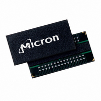
MT41J256M4HX-15E:D TR Micron Technology Inc, MT41J256M4HX-15E:D TR Datasheet - Page 172

MT41J256M4HX-15E:D TR
Manufacturer Part Number
MT41J256M4HX-15E:D TR
Description
IC DDR3 SDRAM 1GBIT 78FBGA
Manufacturer
Micron Technology Inc
Type
DDR3 SDRAMr
Specifications of MT41J256M4HX-15E:D TR
Format - Memory
RAM
Memory Type
DDR3 SDRAM
Memory Size
1G (256M x 4)
Speed
667MHz
Interface
Parallel
Voltage - Supply
1.425 V ~ 1.575 V
Operating Temperature
0°C ~ 95°C
Package / Case
78-FBGA
Organization
256Mx4
Density
1Gb
Address Bus
17b
Maximum Clock Rate
1.333GHz
Operating Supply Voltage (typ)
1.5V
Package Type
FBGA
Operating Temp Range
0C to 95C
Operating Supply Voltage (max)
1.575V
Operating Supply Voltage (min)
1.425V
Supply Current
220mA
Pin Count
78
Mounting
Surface Mount
Operating Temperature Classification
Commercial
Lead Free Status / RoHS Status
Lead free / RoHS Compliant
- Current page: 172 of 208
- Download datasheet (13Mb)
Figure 94: WRITE (BC4 OTF) to PRECHARGE
DQ Input Timing
PDF: 09005aef826aa906
1Gb_DDR3_SDRAM.pdf – Rev. J 05/10 EN
Command 1
DQS, DQS#
Address 3
DQ 4
CK#
CK
WRITE
Bank,
Col n
T0
NOP
T1
Notes:
Figure 85 (page 166) shows the strobe to clock timing during a WRITE. DQS, DQS# must
transition within 0.25
mask setup and hold timings are measured relative to the DQS, DQS# crossing, not the
clock crossing.
The WRITE preamble and postamble are also shown here. One clock prior to data input
to the DRAM, DQS must be HIGH and DQS# must be LOW. Then for a half clock, DQS is
driven LOW (DQS# is driven HIGH) during the WRITE preamble,
must be kept LOW by the controller after the last data is written to the DRAM during the
WRITE postamble,
Data setup and hold times are shown. All setup and hold times are measured from the
crossing points of DQS and DQS#. These setup and hold values pertain to data input
and data mask input.
Additionally, the half period of the data input strobe is specified by
1. NOP commands are shown for ease of illustration; other commands may be valid at
2. The write recovery time (
3. The BC4 setting is activated by MR0[1:0] = 01 and A12 = 0 during the WRITE command
4. DI n = data-in for column n.
5. BC4 (OTF), WL = 5, RL = 5.
NOP
T2
these times.
fies the last burst WRITE cycle until the PRECHARGE command can be issued to the same
bank.
at T0.
WL = 5
NOP
T3
t
WPST.
t
CK of the clock transitions as limited by
NOP
T4
t WPRE
t
172
WR) is referenced from the rising clock edge at T9.
NOP
T5
DI
n
n + 1
DI
Micron Technology, Inc. reserves the right to change products or specifications without notice.
n + 2
NOP
T6
DI
1Gb: x4, x8, x16 DDR3 SDRAM
n + 3
DI
t WPST
NOP
T7
Indicates A Break In
Time Scale
© 2006 Micron Technology, Inc. All rights reserved.
t
NOP
DQSS. All data and data
T8
t
WPRE. Likewise, DQS
t
Transitioning Data
DQSH and
NOP
T9
t WR 2
t
WR speci-
t
DQSL.
Don’t Care
Valid
PRE
Tn
Related parts for MT41J256M4HX-15E:D TR
Image
Part Number
Description
Manufacturer
Datasheet
Request
R

Part Number:
Description:
Manufacturer:
Micron Technology Inc
Datasheet:

Part Number:
Description:
Manufacturer:
Micron Technology Inc
Datasheet:

Part Number:
Description:
IC SDRAM 64MBIT 133MHZ 54TSOP
Manufacturer:
Micron Technology Inc
Datasheet:

Part Number:
Description:
IC SDRAM 64MBIT 5.5NS 86TSOP
Manufacturer:
Micron Technology Inc
Datasheet:

Part Number:
Description:
IC SDRAM 64MBIT 200MHZ 86TSOP
Manufacturer:
Micron Technology Inc
Datasheet:

Part Number:
Description:
IC SDRAM 64MBIT 133MHZ 54TSOP
Manufacturer:
Micron Technology Inc
Datasheet:

Part Number:
Description:
IC SDRAM 128MBIT 133MHZ 54TSOP
Manufacturer:
Micron Technology Inc
Datasheet:

Part Number:
Description:
IC SDRAM 256MBIT 133MHZ 90VFBGA
Manufacturer:
Micron Technology Inc
Datasheet:

Part Number:
Description:
IC SDRAM 128MBIT 133MHZ 54TSOP
Manufacturer:
Micron Technology Inc
Datasheet:

Part Number:
Description:
IC SDRAM 256MBIT 133MHZ 54TSOP
Manufacturer:
Micron Technology Inc
Datasheet:

Part Number:
Description:
IC DDR SDRAM 512MBIT 6NS 66TSOP
Manufacturer:
Micron Technology Inc
Datasheet:

Part Number:
Description:
IC SDRAM 128MBIT 167MHZ 86TSOP
Manufacturer:
Micron Technology Inc
Datasheet:

Part Number:
Description:
IC SDRAM 128MBIT 143MHZ 86TSOP
Manufacturer:
Micron Technology Inc
Datasheet:

Part Number:
Description:
SDRAM 256M-BIT 1.8V 54-PIN VFBGA
Manufacturer:
Micron Technology Inc
Datasheet:

Part Number:
Description:
IC SDRAM 128MBIT 143MHZ 86TSOP
Manufacturer:
Micron Technology Inc
Datasheet:


