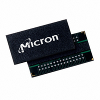
MT41J256M4HX-15E:D TR Micron Technology Inc, MT41J256M4HX-15E:D TR Datasheet - Page 141

MT41J256M4HX-15E:D TR
Manufacturer Part Number
MT41J256M4HX-15E:D TR
Description
IC DDR3 SDRAM 1GBIT 78FBGA
Manufacturer
Micron Technology Inc
Type
DDR3 SDRAMr
Specifications of MT41J256M4HX-15E:D TR
Format - Memory
RAM
Memory Type
DDR3 SDRAM
Memory Size
1G (256M x 4)
Speed
667MHz
Interface
Parallel
Voltage - Supply
1.425 V ~ 1.575 V
Operating Temperature
0°C ~ 95°C
Package / Case
78-FBGA
Organization
256Mx4
Density
1Gb
Address Bus
17b
Maximum Clock Rate
1.333GHz
Operating Supply Voltage (typ)
1.5V
Package Type
FBGA
Operating Temp Range
0C to 95C
Operating Supply Voltage (max)
1.575V
Operating Supply Voltage (min)
1.425V
Supply Current
220mA
Pin Count
78
Mounting
Surface Mount
Operating Temperature Classification
Commercial
Lead Free Status / RoHS Status
Lead free / RoHS Compliant
- Current page: 141 of 208
- Download datasheet (13Mb)
Mode Register 3 (MR3)
Figure 59: Mode Register 3 (MR3) Definition
MULTIPURPOSE REGISTER (MPR)
PDF: 09005aef826aa906
1Gb_DDR3_SDRAM.pdf – Rev. J 05/10 EN
Notes:
With dynamic ODT (R
to dynamic ODT (R
back to ODT (R
R
namic ODT (R
and
Dynamic ODT is only applicable during WRITE cycles. If ODT (R
namic ODT (R
one other. Dynamic ODT is not available during write leveling mode, regardless of the
state of ODT (R
tion (ODT) (page 187).
The mode register 3 (MR3) controls additional functions and features not available in
the other mode registers. Currently defined is the MULTIPURPOSE REGISTER (MPR).
This function is controlled via the bits shown in Figure 59 (page 141). The MR3 is pro-
grammed via the LOAD MODE command and retains the stored information until it is
programmed again or until the device loses power. Reprogramming the MR3 register
will not alter the contents of the memory array, provided it is performed correctly. The
MR3 register must be loaded when all banks are idle and no data bursts are in progress,
and the controller must wait the specified time
sequent operation.
The MULTIPURPOSE REGISTER function is used to output a predefined system timing
calibration bit sequence. Bit 2 is the master bit that enables or disables access to the
MPR register, and bits 1 and 0 determine which mode the MPR is placed in. The basic
concept of the multipurpose register is shown in Figure 60 (page 142).
If MR3[2] is a 0, then the MPR access is disabled, and the DRAM operates in normal
mode. However, if MR3[2] is a 1, then the DRAM no longer outputs normal read data
M15
TT,nom
0
0
1
1
1. MR3[16 and 13:3] are reserved for future use and must all be programmed to 0.
2. When MPR control is set for normal DRAM operation, MR3[1, 0] will be ignored.
3. Intended to be used for READ synchronization.
M14
t
ADC.
0
1
0
1
0 1
16
BA2
value will be High-Z. Special timing parameters must be adhered to when dy-
Mode register set 1 (MR1)
Mode register set 2 (MR2)
Mode register set 3 (MR3)
Mode register set (MR0)
15
1
BA1
Mode Register
1
14
BA0
TT(WR)
TT(WR)
TT,nom
TT,nom
0 1 0 1
13
A13
TT(WR)
12
) is enabled: ODTLcnw, ODTLcnw4, ODTLcnw8, ODTH4, ODTH8,
) is still permitted. R
A12 A11
) at the completion of the WRITE burst. If R
). For details on dynamic ODT operation, refer to On-Die Termina-
TT(WR)
0 1 0 1 0 1 0 1
11
) when beginning a WRITE burst and subsequently switches
10
A10
) enabled, the DRAM switches from normal ODT (R
141
9
A9
M2
0
1
8
A8
Normal DRAM operations 2
0 1
7
Dataflow from MPR
A7 A6 A5 A4 A3
0 1
MPR Enable
Micron Technology, Inc. reserves the right to change products or specifications without notice.
6
TT,nom
0 1 0 1 0 1
5
4
1Gb: x4, x8, x16 DDR3 SDRAM
and R
t
MRD and
3
MPR
2
TT(WR)
A2 A1 A0
MPR_RF
1
Mode Register 3 (MR3)
M1
0
0
1
1
t
MOD before initiating a sub-
can be used independent of
M0
0
0
1
0
1
© 2006 Micron Technology, Inc. All rights reserved.
Predefined pattern 3
MPR READ Function
TT,nom
Address bus
Mode register 3 (MR3)
TT,nom
Reserved
Reserved
Reserved
) is disabled, dy-
is disabled, the
TT,nom
)
Related parts for MT41J256M4HX-15E:D TR
Image
Part Number
Description
Manufacturer
Datasheet
Request
R

Part Number:
Description:
Manufacturer:
Micron Technology Inc
Datasheet:

Part Number:
Description:
Manufacturer:
Micron Technology Inc
Datasheet:

Part Number:
Description:
IC SDRAM 64MBIT 133MHZ 54TSOP
Manufacturer:
Micron Technology Inc
Datasheet:

Part Number:
Description:
IC SDRAM 64MBIT 5.5NS 86TSOP
Manufacturer:
Micron Technology Inc
Datasheet:

Part Number:
Description:
IC SDRAM 64MBIT 200MHZ 86TSOP
Manufacturer:
Micron Technology Inc
Datasheet:

Part Number:
Description:
IC SDRAM 64MBIT 133MHZ 54TSOP
Manufacturer:
Micron Technology Inc
Datasheet:

Part Number:
Description:
IC SDRAM 128MBIT 133MHZ 54TSOP
Manufacturer:
Micron Technology Inc
Datasheet:

Part Number:
Description:
IC SDRAM 256MBIT 133MHZ 90VFBGA
Manufacturer:
Micron Technology Inc
Datasheet:

Part Number:
Description:
IC SDRAM 128MBIT 133MHZ 54TSOP
Manufacturer:
Micron Technology Inc
Datasheet:

Part Number:
Description:
IC SDRAM 256MBIT 133MHZ 54TSOP
Manufacturer:
Micron Technology Inc
Datasheet:

Part Number:
Description:
IC DDR SDRAM 512MBIT 6NS 66TSOP
Manufacturer:
Micron Technology Inc
Datasheet:

Part Number:
Description:
IC SDRAM 128MBIT 167MHZ 86TSOP
Manufacturer:
Micron Technology Inc
Datasheet:

Part Number:
Description:
IC SDRAM 128MBIT 143MHZ 86TSOP
Manufacturer:
Micron Technology Inc
Datasheet:

Part Number:
Description:
SDRAM 256M-BIT 1.8V 54-PIN VFBGA
Manufacturer:
Micron Technology Inc
Datasheet:

Part Number:
Description:
IC SDRAM 128MBIT 143MHZ 86TSOP
Manufacturer:
Micron Technology Inc
Datasheet:


